Design of single user tracking in WRNC system
This paper introduces a mechanism to enable the RNC (Radio Network Control) within the radio network controller to easily and accurately collect the statistical information of each link in the single-user data processing, so that the single-user information can be quickly counted and checked to improve the problem Analysis efficiency.
With the rapid development of 3G networks, WCDMA systems are being commercialized on a large scale. In the past, some commonly used positioning methods, such as breakpoint debugging and LogView, have become increasingly difficult to meet the needs of the field. Compared with the simple laboratory environment, the field positioning problem will be more difficult. At present, for the instability of HSDPA / HSUPA service rate and the failure of PS service (Packet Stream data service), the common troubleshooting methods are very limited, and the positioning is very difficult. . In addition to the special circumstances of many users in the field and large interference data, the traditional positioning method simply cannot obtain the relevant statistical information and traffic tracking information of a single user, which brings many difficulties to the location and resolution of the problem.
1 The occurrence and phenomenon of rate problems
There are three main reasons for the internal rate problem of RNC: (1) improper processing of data packets by the user plane and abnormal packet loss; (2) the connection parameters passed to the user plane by the control plane are incorrect, and the user plane and the bearer cannot be connected; (3 ) The user plane itself is not properly handled when handling various connection relationships.
In practical applications, the rate phenomena in several different situations are as follows: (1) the upstream and downstream rates are unstable when the HSDPA / HSUPA service is running; (2) the rate decoupling occurs during the HSDPA / HSUPA service; (3) HSDPA / HSUPA The PS service cannot reach the contracted expected rate; (4) The rate is normal.
2 Traditional positioning methods and defects
At present, the traditional rate positioning method is divided into three types: SHELL command positioning, DSP printing positioning and signaling tracking positioning.
But for field positioning, these traditional positioning methods are difficult to achieve. First of all, the SHELL command positioning, the number of field interface boards is large, and carries different services. It is extremely troublesome to enter the SHELL commands in turn between the interface boards. At the same time, the SHELL command can only track all business traffic information, and cannot target specific users. Lack of pertinence. Secondly, the external field has strict requirements for printing. Generally, it is not allowed to open internal printing. The official commercial bureau has relatively few resources. Opening a lot of internal printing will affect the operation of the entire system. Finally, the signaling tracking only records the basic information of the control plane, and cannot really help the user plane inspection.
Therefore, for such problems, a good positioning method is needed to lock the problem to the specific interface or FP level. Single-user tracking is designed for this defect, and its advantages are: (1) Data reporting is recorded through background signaling tracking, which is conducive to observation; (2) Data tracking uses FP as the unit to directly locate the business channel and locate accurately ; (3) No additional overhead is added to normal equipment operation, and no extra manual operation is required, which is convenient to use.
3 Design and implementation of single user tracking
3.1 Overall overview of WCDMA system
The WCDMA system is mainly composed of three core parts, which are divided into a core network (CN), a radio network controller (RNC) and a base station (NodeB). RNC connects CN and NodeB and plays an important role in WCDMA. The IUR port is used to connect RNC and RNC. RNC is divided into three parts: CRNC (control RNC), SRNC (service RNC) and DRNC (drift RNC) [5].
3.2 Data flow tracked by a single user
The path of the data flow in the RNC is divided into two, one is to directly enter the SRNC through the IUB port, and reach the CN through the IU port; the other is to reach the DRNC through the IUB port, then from the DRNC to the SRNC through the IUR port, and finally reach the CN [6] . If you can count the data packets of each FP at each node and compare the data traffic of each node, you can quickly locate the data loss interface and FP.
3.3 Overall design of single user tracking
The protocol architecture of each interface of UTRAN is designed according to a common protocol model, as shown in Figure 1. The design principle is that the floors and planes are logically independent of each other. From a horizontal perspective, the protocol structure mainly includes two layers: the wireless network layer and the transmission network layer. All UTRAN related issues are only related to the wireless network layer, and the transport network layer is only the standardized transmission technology adopted by UTRAN, and has nothing to do with the specific functions of UTRAN. Viewed from the vertical plane, the protocol structure includes control plane, user plane, transmission network control plane and transmission network user plane [1]. 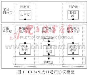
This design is divided into the following modules according to the protocol architecture of UTRAN: message processing module, control plane, user plane, bearer management module and signaling tracking module.
The entire single-user tracking design idea is shown in Figure 2, where the solid line represents the control flow and the dotted line represents the data flow. 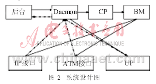
For control information, the task of tracking the media plane is distributed to the message processing module (Daemon), and Daemon notifies the control plane CP (Control Plane) and the user plane UP (User Plane). The control plane notifies the bearer management module BM (Bear Management, BM) to establish and delete related bearer tracking when the bearer link is established and deleted. Extract relevant information from the message and send a message to inform the interface board. After receiving the message, the interface board sets the filtering conditions and performs filtering statistics on the processed messages.
For the data service flow, after collecting the tracking information, the interface board and the user plane directly report the tracking information to Daemon. Daemon will check the content of the message and report it to the background.
3.4 Implementation process of single user tracking
In order to successfully realize the traffic reporting of each interface FP under the framework of the existing system, the following two processes are designed: task start and data reporting and verification.
3.4.1 Start of single user tracking on the media
The start-up process for single-user tracking is:
(1) The background sends an EV_UE_MEDIA_START_REQ request message to the signaling tracking module (ToolKit). The message carries the IMSI number and tracking flag to be tracked to ToolKit.
(2) ToolKit adopts a response processing mechanism. After receiving the message, it immediately responds to the background, notifying that the message has been received. ToolKit maintains a state table (TraceUE) about various tracking tasks of UE. Judging from the IMSI number in the message, if the saved IMSI number cannot be queried in the ToolKit module, it indicates that the process is wrong and the process ends directly. If the IMSI number exists and is already in the tracking state, it means that the tracking is repeated and ends directly. If the IMSI number is in an untracked state, ToolKit will create a context about the UE and save it in the TraceUE information for future query and use.
(3) ToolKit needs to send a message EV_START_MEDIA_TRACE to the message processing module (Daemon). Daemon decides which modules need to send trace messages according to different messages.
(4) Daemon sends a message EV_START_MEDIA_TRACE to the media plane to the user plane. After receiving the tracking instruction message, the user plane records the tracking information, so that when the bearer interface is called to establish the connection table, it indicates that the data on the bearer link needs to be tracked, so that the data amount information can be directly reported from the user plane.
(5) Daemon sends an EV_START_MEDIA_TRACE message to each terrestrial interface (IUB / IUR / IU), triggering each terrestrial interface to send tracking instructions to its respective underlying link.
(6) After receiving the tracking message of the media single user, each terrestrial standard module searches for the transport layer information about the UE according to the IMSI number, starts the message sending mechanism, and then carries the bearer related to the UE to the bearer management The module sends an EV_START_LINK_TRACE message to trigger that the underlying bearer about this UE is marked as tracking. This message not only needs to carry all the information (BearId, bindingID, TransportAddress, etc.) when the bearer link is established, but also adds the flag bit tracked by the media plane. After receiving the message, the underlying bearer management module BM needs to traverse and check the bearer information, and mark the relevant fields of the bearer link that really needs to be tracked, which is convenient for later statistics.
3.4.2 Reporting time and verification of single user tracking on media
(1) Reporting time alignment
The reporting of data is the result of accumulation within a certain period of time. In order to ensure the accuracy of business data statistics, it is necessary to ensure the consistency of the system time on each board. To ensure this, the strategy of aligning the initial zero clearing time and the statistical reporting time is adopted.
Statistic initial clearing time alignment: When the bearer link is established, the interface board clears the statistical information corresponding to this link. The user plane processing board also uses a similar method to clear statistics on related bearers.
The time alignment of statistical reporting is implemented in two ways: (1) The granularity of reporting is agreed, for example, 15 s, 30 s, 60 s, etc. (2) Align by the absolute time on the board. For example, on the premise of time alignment, report at 15 s, 30 s, 45 s, and 60 s per minute. In order to align the reporting time, a new soft clock that records absolute time is maintained on the DSP. The soft clock reference is synchronized by HOST, which can periodically correct the clock on the DSP.
(2) Reporting channels
In order to check the information, two reporting methods are designed: (1) There are keep-alive messages between each interface module of the CP and the UP, and the keep-alive messages will trigger the UP to report all the users on different interfaces (IUB, IUR, IU) Statistics of the bearer link. After receiving the keep-alive message, UP finds that the user is being tracked by the media plane, and then calls the data reporting interface to report statistics. At this time, the user plane will query the bearer information that was tracked at startup. Through the internal mechanism, the tracking information is forwarded to Daemon until it is sent to the background. (2) When each CP interface module sends a keep-alive message to the UP and finds that the user is being tracked by the media, it sends a data report request message EV_START_LINKTRACERPT_REQ to the BM module. After receiving the message, the BM will notify the user according to the locally saved tracking user information. Interface board. The interface board reports the tracking information to Daemon until the background.
(3) Check of statistical information
When the user plane calls the bearer interface to send packets, it will filter based on the information of the bearer tracked in the interface. When receiving a message, the message is filtered according to the information in the bearer connection table.
For the interface board, the bearer management module needs to set filtering conditions on the statistical information. For different load types, the filter conditions are inconsistent. In the ATM mode, IUB, IUCS, and IUR need to filter the information of incoming and outgoing network elements based on the information of VPI, VCI, and CID, and IUPS needs to complete the filtering of incoming and outgoing calls based on the TEID of the opposite end and the local end. In IP mode, IUB, IUCS, and IUR complete the filtering of incoming and outgoing network elements based on the local IP address and UDP port number. IUPS requires the TEID of the local and peer to determine.
In order to check the statistical information with the user plane, for each bearer link, the control plane also needs to inform the bearer management module of the filtering direction, interface type, link attributes and global identification information of the user.
Daemon summarizes and checks the data reported by the two channels to prevent inconsistency of statistical information and improve the accuracy of information reporting.
4 Test results of single user tracking
This design has been tested and verified in the WRNC system. Figure 3 is the signaling analysis of the Iu port in the service report message. 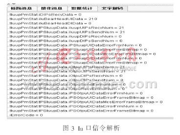
This includes some statistical cells tracked by a single user. Such as: IuupUlPsRecvNum, IuupUlPsSendNum, IuupDlPsRecvNum and Iuup DlPsSendNum, etc., respectively record the amount of data sent and received in the upstream and downstream PS domain. From the figure, it can be seen that the upstream sending and receiving data volume of IuUp is 21, which means that the data sending and receiving of this FP is normal, and there is no abnormal situation.
It can be seen from Figure 3 that the solution successfully collects and reports business data. The signaling trace in the background clearly records the type and data of each FP in each standard interface.
This solution realizes the reporting and statistics of user data of each interface within the RNC, and completely solves the complexity and inaccuracy of traditional rate problem positioning. The accurate positioning, easy observation and easy operation make the positioning method much better than the traditional positioning method.
In the application of the commercial bureau, single-user tracking can greatly shorten the positioning time of the rate problem and greatly reduce the interference of other users in the field. This design has played an important role in improving operator satisfaction and rapidly advancing the deployment of 3G in China.
The Single Most Important Thing You Need To Know About Single Sided PCB
As a single sided PCB manufacturer, Jinghongyi PCB has been single sided PCB for many years. Production and manufacturing experience, with a very exquisite single sided PCB Manufacturing process flow chart.
We can produce single sided copper PCB, single sided copper clad PCB Board , single sided Flex PCB .
We know that when you choose single sided PCB manufacturer, product quality is one of the first factors you need to consider. We are not only engaged in PCB manufacturing for many years, but also one of the large-scale PCB manufacturers in China. We can not only produce single sided PCB, but also Double Sided PCB , Multilayer PCB , Aluminum PCB and so on.
In addition to product quality, you may also need to consider the single sided PCB price factor. If you choose us as your partner, you can rest assured that we will be able to provide you with not the best price on the premise of guaranteeing product quality, but the price that we both feel is very reasonable. What do you think?
In this article, we will elaborate on the definition, type, cost components, structure, advantages and disadvantages, manufacturing process and raw materials of single sided PCB. Finally, we will introduce the application of single sided PCB and the differences between single sided PCB and double sided PCB. And how to choose between single sided PCB and double sided PCB.
What Is Single Sided PCB

Single-sided PCB diagram mainly used Network Printing(Screen Printing), that is, resist on copper surface, After etching, mark the welding resistance, and then finish the hole and the shape of the part by punching.
Fundamentally, single-sided and double-sided Printed Circuit Boards serve the same purpose. Both serve as catalysts for electrical connections between components, however there are some key differences that set them apart from each other. More specifically, they differ in the costs associated with production and development processes, as well as ampacity differences.
With the appearance of electronic transistor, single sided PCB was developed in the early of 1950, which is mainly manufactured in USA. Single-sided PCB was manufactured by copper etching directly at that time. During 1953 to 1955, Japan use imported copper make out paper phenolic aldehyde copper substrate, and apply mainly on radio products. In 1956, single-sided PCB technology was made big progress with the appearance of professional PCB manufacturers from Japan. In the early stage, copper substrate mainly used paper phenolic aldehyde, but because paper phenolic aldehyde with the factors of low electric insulation, bad solder thermal stability, twist issue etc, paper epoxide resin and glass fiber epoxy resin was developed soon after. Currently, paper epoxide resin is widely used in consuming electronic.
Basically, there is no challenge for PCB manufacturer to produce single sided PCB and the technology is quite mature nowadays. The main focus for PCB manufacturer is how to control production cost and save more cost for customers.
Types of Single Layer PCB
- Single Layer Rigid PCB
It is the type of a single layer PCB which is made up a rigid material such as fiber glass. These PCBs are inflexible and prevent the circuit from bending and breaking. Currently these are used in different types of devices such as in calculators and power supplies etc.
- Single Layer Flexible PCB
It is the type of a single layer PCB which is mode out a flexible material instead of a rigid material and for this purpose plastic materials are used. It has so many advantages over single layer rigid pub but it fabrication cost is so much high.
- Single Layer Rigid Flex PCB
It is the type of a single layer PCBs which is used for high frequency circuits normally in giga hertz. These PCBs are made out a Teflon or polyphenylene oxide (PPO) material. During choosing high frequency single layer PCB many aspects are keep in mind such as dielectric loss, thermal expansion and water absorption etc.
- Single Layer High Frequency PCB
It the type of single layer PCBs which is made out by the combination of plastic and fiber glass. Both materials are combined together into single layer. It has so many advantages over single layer rigid and flexible PCB such as it reduces the weight and size of overall PCB.
- Single Layer Aluminum PCB
What Goes Into Determining single sided PCB Costs and price
No matter whether manufacturing a single-sided PCB, double-sided PCB, or multilayer PCB, three main cost categories exist: Primary production costs, dependent costs, and overhead costs.
Often, single layer PCB are used for simple devices and usually cheaper than multilayer PCB.
Multilayer PCB has one or multiple conductor patterns inside the board, this increases the area available for wiring. multilayer PCB, such as 4 Layer PCB , 6 Layer PCB and 8 Layer PCB are usually used for more complicated devices. For example, smart phones use 12 layers due to the various demands of the circuit. As a result, multilayer PCB circuit boards are more expensive.
You can break them down into the following categories:

Layout alters the cost balance. While the number and size of holes remain the same with single-sided PCBs, two different circuit designs on one substrate change the number of holes and add vias.
Because double-sided PCBs welcome complex circuit designs, layout also becomes a dependent factor. As the number of traces increase, costs increase. Smaller surface mount components fastened to the bottom side change the trace spacing. As the space between the traces narrows, costs can jump 5 to 10 percent.
Different layouts may require different hole sizes and the use of laser rather than mechanical drills. Smaller hole sizes and larger hole counts drive the cost higher because of a change in the manufacturing process.
Advantages of Single Sided PCB

- Simple and easy to design and install
- Lower cost, especially for high volume orders
- Easy drilling, soldering, de-soldering and components inserting process
- Lower probability of manufacturing issues,such as short circuiting and producing noise
- Components are installed at only one side, require lower jumper to compensate the circuit
- Popular, common, and easily understood by most PCB manufacturers
- Less time for fault tracing and repairing
Single Layer PCB Disadvantages
Despite their cost advantages and other perks, single-layer boards are not the right choice for every project due to the limitations they have, which include:
- Simplistic Design: The simplicity of single-layer boards' is one of their biggest benefits, but it's also a substantial limitation. For more complex devices that require a higher number of components and connections, a single layer does not provide enough space or power. If wires cross each other, the device won't function properly, so it's critical that the board has enough space to accommodate everything. More complex designs just can't fit on single-sided PCBs.
- Slower Speed and Lower Operating Capacity: The limited number of connections on these boards also affects their power and speed. These less-dense designs are not as robust as those with more circuits and have a lower operating capacity. They might not have enough power for some applications.
- Larger Size and Higher Weight: To add capabilities to a single-sided board, you need to expand its dimensions rather than add another layer, as you could with you a multi-layer PCB. You could use multiple separate boards, but one multi-layer board could likely handle the same requirements. Increasing the size or number of boards in a device also increases your final product's weight.
How to make single sided PCB

Single sided PCB manufacturing Process flow chart
One thin layer of thermally conductive but electrically insulating dielectric is laminated with copper. Soldermask is usually applied on top of the copper.
Cutting - Cleaning - Drilling - Cleaning - PTH - Panel - Plating - Cleaning - Photolithography - Image Transfer - Inspection - Copper/Tin - Plating - Coating - Removing/Etching/Tin - Removing - Inspection - Cleaning - Solder - Mask - Exposure/Develop/Inspection - Prepreg - Screen - HASL - Conformal - Coating - Post - Soldering - Cleaning - Test - Final Inspection - Packing
Single layer PCB Raw Material
- Fr4 Grade Fiberglass Laminates
- Aluminum
- Copper base
- Cem 1
- Cem 3
Construction of Single Sided PCB


The base material, which is also named as substrate, is composed of insulating fiber glass which gives PCB strength and compact look. The nature and type of base material defines if board is going to be Flexible PCB or Rigid PCB.
Above substrate, there lies a copper layer which provides conducting path for various components on the board. The copper thickness is different for different boards depending on your needs and requirements and is defined in ounces per square foot.
On the top of copper foil, there exists a solder mask layer. This layer is mainly used for protection and makes the copper foil insulating which helps in avoiding the conduction in case direct contact happens with some conducting material.
On the top of all layers, there exists a silkscreen layer that is mainly used for adding symbols and characters on the board so a common person can anticipate the clear understanding of the board.
Single Sided PCB Applications

- Vending machines
- Camera systems
- Surveillance
- Calculators
- Printers
- Solid state drives
- Coffee makers
- LED lighting
- Packaging equipment
- Sensor products
- Power supplies
- Relays
- Radio and stereo equipment
- Timing circuits
What Is Double Sided PCB

It need circuits on both sides. Via is the holes on boards, coated with metal and it can connect wires on both sides. Because the area of Double-sided PCB is twice as large as the Single-sided PCB, and because the wiring is interleaved, which is better suited for circuits that are more complex.
Someone may feel confused that if one Double-sided PCB, wires on both sides while Electronic parts only one side, is this a Double-sided board or a single onel? The answer is obvious. This kind of board is a Double-sided board, it's just install a component on the Double-sided board.
Differences Between Single sided PCB and Double sided PCB

single sided vs double sided PCB
Single and double sided printed circuit boards share the same material make-up: FR-4, which is a form of fiberglass mixed with epoxy. In modern manufacturing, this is usually layered with copper for conductivity and then coated in solder mask for a professional finish. Sometimes, in a process called silk screening, industrial printers print markings and labels on the board as well.
Single-sided PCBs consist of the FR4 insulating core substrate and a thin layer of copper coating on the bottom or solder-side of the substrate. Through-hole components mount on the top or component-side of the substrate with the leads passing through to the bottom side and soldered to the copper pads and tracks. Surface mount components mount directly to the solder side. The primary difference between the two boards will be in conductor placement.
Double-sided boards rely on the same core substrate but have conductors on both sides of the substrate. Very simply, a double-sided board delivers twice the area for conductors. Complex routing can occur with through-hole components mounted on the top layer and surface mount components mounted on the bottom layer. Plated through holes establish [vias" or the electrical connections between the two sides.
Choose Single Sided PCB or Double Sided PCB?
Which PCB you pick depends on your needs and requirements. Sometimes single sided PCBs are more suitable for project design as compared to double sided PCBs and vice versa.
Before you pick any type of PCB for your project, you must take one thing into consideration that single sided PCB layouts are more difficult to route as compared to double sided PCB, but following are the reasons why you should put an effort for making and picking single sided PCB over other PCBs.
- If you are hobbyist or students, and concerned to make PCB at home, you must know, developing single sided PCBs at home are much easier than developing double sided PCBs at home.
- As you are a manufacturer and very much interested to keep your cost down and producing a single sided PCB a most economical process. In terms of cost, producing single sided PCBs are more economical than producing double sided PCBs.
- Almost all HVAC systems make use of single sided PCBs, because they are more reliable and cost effective and don`t compromise the overall quality of the product.
- Using through hole technology in single sided PCBs still have its drawbacks and limitations because conductive layers, lines and pads stay on single side of PCB but it still is a cheap process to combine all components at one place. Multilayer PCB is also used in many applications where single sided and double sided PCBs fail to fulfill the requirements.
Relationship Resources
Multilayer Metal Core PCB
Single Layer Metal Core PCB
Single Sided Flexible PCB
Single Sided PCB
Single Sided PCB, Single Layer PCB, 1 Layer PCB, making circuit boards
JingHongYi PCB (HK) Co., Limited , https://www.pcbjhy.com