Hardware Design of Universal Wireless Sensor Network Based on ZigBee
introduction
As an emerging technology, wireless sensor network has become a hotspot of research at home and abroad, and it has shown broad application prospects in military, environmental, health, family, commercial, space exploration and disaster relief fields [1]. Many units at home and abroad have carried out research in related fields, but most of the work is still in the wireless network protocol performance simulation and hardware node small-scale experimental design stage. Wireless sensor networks do not require high transmission bandwidth, but require extremely low power consumption, so that devices in wireless sensor networks can work longer, and low cost is also a major requirement for the popularization of wireless sensors. The ZigBee / IEEE 802.15.4 standard takes low power consumption and low cost as the main goals, and provides a platform for wireless sensor networks to interconnect with each other. At present, research and development of wireless sensor networks based on this technology have received more and more attention. This article is based on ZigBee technology, designed a universal wireless sensor network hardware platform, in order to look forward to industrialization, and make greater contributions to China's wireless sensor business.
Main advantages of wireless sensor network based on ZigBee
The word ZigBee comes from the bees swarming the position of the pollen, by dancing Z-shaped dance to inform the companions, to achieve the purpose of exchanging information. It can be said that a small animal achieves "wireless" communication in a simple way. People call this a short-range wireless network communication technology that focuses on low power consumption, low cost, low complexity, and low rate. . ZigBee technology is not a completely unique and completely new standard. Its physical layer, MAC layer and link layer adopt the IEEE 802.15.4 standard, but on this basis, it has been improved and expanded. The network layer, application convergence layer and high-level application specifications are formulated by the ZigBee Alliance. ZigBee has outstanding characteristics, especially in low power consumption and low cost, mainly in the following aspects [2].
â‘ Low power consumption. In the low-power standby mode, two No. 5 dry batteries can support one node to work for 6 to 24 months, or even longer. This is ZigBee's outstanding advantage. In comparison, Bluetooth can only work for a few weeks, and WiFi can only work for a few hours.
â‘¡ Low cost. By greatly simplifying the protocol (less than 1/10 of Bluetooth), the requirements for the communication controller are reduced. According to predictive analysis, the 8051 8-bit microcontroller is used for calculation. The full-function master node requires 32 KB code, and the sub-function node As little as 4 KB code, and ZigBee is free of agreement patent fees.
â‘¢ Low rate. ZigBee works at a lower rate of 20 to 250 kbps, providing raw data throughput rates of 250 kbps (2.4 GHz), 40 kbps (915 MHz) and 20 kbps (868 MHz), respectively, to meet the application requirements of low-rate transmission data.
â‘£ Up close. The transmission range is generally between 10 and 100 m. After increasing the RF transmission power, it can also be increased to 1 to 3 km. This refers to the distance between adjacent nodes. If the relay is used for routing and communication between nodes, the transmission distance can be farther.
⑤ Short delay. ZigBee's response speed is relatively fast, generally only 15 ms to switch from sleep to working state, and only 30 ms to connect the node to the network, which further saves energy. In comparison, Bluetooth requires 3 to 10 s and WiFi requires 3 s.
â‘¥ High capacity. ZigBee can adopt star, sheet and mesh network structure, a master node manages several child nodes, and at most one master node can manage 254 child nodes; at the same time, the master node can also be managed by the upper layer network node, which can form up to 65 000 A large network of nodes.
⑦ Simple agreement and high security. The ZigBee protocol stack has an average length of only 1/4 of Bluetooth. This simplification is very important for low cost, interoperability, and maintainability. ZigBee technology provides data integrity check and authentication functions, and provides a three-level security mode, which can flexibly determine its security attributes, and network security can be effectively guaranteed.
⑧ Free license band. Direct sequence spread spectrum is used in the Industrial Scientific and Medical (ISM) band—2.4 GHz (global), 915 MHz (United States) and 868 MHz (Europe).
From the main technical characteristics of ZigBee mentioned above, it can be seen that based on the IEEE802.15.4 standard, coordinated communication between thousands of tiny sensors can be achieved. In addition, the relay method is used to transmit data from one sensor to another through radio waves, which can make the communication efficiency very high. Compared with various existing wireless communication technologies, ZigBee technology's low power consumption and low rate are most suitable for wireless sensor networks.
Wireless sensor network hardware design
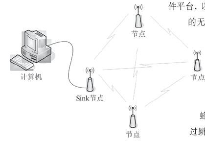
In wireless sensor networks, nodes are scattered randomly in the monitored area. The nodes form a network in a self-organizing manner, and transmit the monitoring data to the Sink node through multi-hop relay. Finally, the data in the entire area is transmitted to the remote center for centralized processing by means of a long-distance or temporarily established Sink link. Figure 1 shows the general form of wireless sensor network architecture [3].

For environmental and structural condition monitoring, we have designed a universal wireless sensor network hardware platform, which consists of several sensor nodes, Sink nodes with wireless receiving function, and a computer. The wireless sensor nodes are distributed in the area to be monitored, and perform data collection, processing, and wireless communication. The Sink node receives data from each sensor and transmits the data to the computer in a wired manner, as shown in Figure 2.
Hardware design of wireless sensor node
The wireless sensor node is generally composed of four parts: a sensor module, a data processing module, a data transmission module and a power management module. Among them, the sensor module is responsible for collecting the information of the monitoring area and completing the data conversion. The collected information can include temperature, humidity, light intensity, acceleration, and atmospheric pressure; the data processing module is responsible for controlling the processing operations, routing protocols, synchronous positioning Power consumption management and task management, etc .; the data transmission module is responsible for wireless communication with other nodes or Sink nodes, exchange control messages and send and receive data collection; the power management module selects the sensors used, and the node power supply uses micro button batteries to reduce The volume of the node.
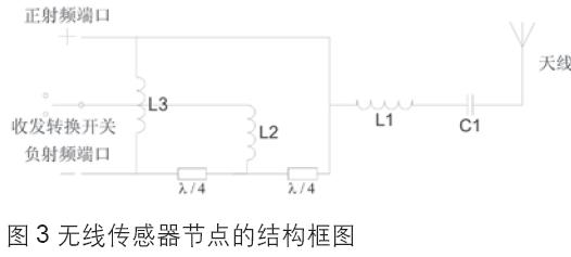
The node realization mechanism we designed is to replace the traditional serial communication module with ZigBee transmission module, and send the collected information data wirelessly. The node includes ZigBee wireless transmission module, microcontroller module, sensor module and interface circuit, DC power module and external memory. In order to reduce the cost of the sensor node and the volume of the sensor node, we use the highly integrated SoC chip CC2430 from Chipcon to implement the data transmission and processing functions of the sensor node. Figure 3 is a structural block diagram of the designed wireless sensor node. The following will introduce several main functional modules in the wireless sensor node.
SoC chip CC2430
The CC2430 chip continues the architecture of the previous CC2420 chip, integrating the ZigBee RF front end, memory, and microcontroller on a single chip. It uses an 8-bit 8051 MCU with 128 KB of programmable flash memory and 8 KB of RAM. It also contains an analog-to-digital converter (ADC), several timers (TImer), AES128 coprocessor, watchdog timer, Sleep mode timer, power-on reset circuit, power-down detection circuit for 32 kHz crystal, and 21 programmable I / O pins. The CC2430 chip is produced using a 0.18 μm CMOS process, and the current consumption during operation is 27 mA; in the receiving and transmitting modes, the current consumption is lower than 27 mA or 25 mA, respectively. The CC2430's sleep mode and ultra-short time transition to active mode are particularly suitable for applications that require very long battery life.
Thanks to the high integration of CC2430, its peripheral circuits are very simple, requiring only a small number and inexpensive peripheral components to complete the data transmission and processing functions of the wireless sensor node, thus greatly reducing costs.
Sensor module
Choose different sensors to detect physical signals such as temperature, humidity, vibration, sound and light in the monitoring area according to actual needs. Optional photosensors, digital format sensors and electret microphones are used to detect light intensity, temperature, vibration and sound.
Photoresistor 5516 is a light pipe that works based on the semiconductor photoelectric effect, and its sensitivity to light intensity is quite high. When exposed to a certain wavelength range, its resistance (bright resistance) decreases sharply, the current increases rapidly, and the voltage is divided by a reference resistor After the analog-to-digital conversion, the resistance of the photoresistor can be obtained, and then the light intensity can be converted.
Maxim's DS18B20 is a one-line digital temperature sensor. The measurement result can be selected from 9 to 12 bit serial data output. The measurement range is -55 to 125 ° C, and the measurement accuracy is ± 0.5 ° C at -10 to 85 ° C.
The electret microphone HX034P is a condenser micro microphone. The input signal is a sound signal, and the output signal is sampled by A / D of the voltage value after the pre-amplifier circuit formed by MAX4466. The A / D sampling frequency of the processor can reach 200KHz, and the sound signal can be captured.
ADI's ADXL202 is a biaxial acceleration sensor, which uses advanced micro-electromechanical system technology, etched a polysilicon coded micromechanical sensor in the same silicon chip, integrated precision signal processing circuit, can measure static and dynamic acceleration. The sensor can be widely used in inertial navigation, earthquake monitoring, vehicle safety and motion status testing of battery-powered equipment.
The wireless sensor network node using a combination of the above sensors and sensitive devices can achieve accurate measurement and detection of temperature and acceleration (vibration). The photoresistor has its own spectral characteristics and temperature characteristics, so it is not accurately calibrated in the design; in addition Acquiring and reproducing sound signals requires a lot of data processing. From the perspective of energy utilization and streamlining of sensor node functions, the detection of sound and light intensity in the design provides a Boolean output by setting a threshold.
Power module
To achieve the miniaturization of the node design, the node can be powered by the rechargeable lithium ion button battery LIR2032 with an output voltage of 3.6V. The self-discharge rate of this type of battery is less than 10% per month, but the rated capacity is small, which limits the lifetime of the node. If it is powered by two No. 5 batteries, it can maintain a longer working time and work in a network. By properly setting the receiving, transmitting and standby states of the node emitter, the service life of the node can be effectively extended. Aiming at the wireless sensor network where the node power supply unit is not easy to replace, the research on new energy solutions and the low-power design of the network system are also topics that deserve attention.
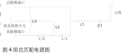
Impedance matching network
The radio frequency signal of CC2430 adopts the differential way, its optimal differential load impedance is 115 + j180Ω, the impedance matching circuit needs to be adjusted according to this value. This design uses a 50-ohm monopole antenna. Because the RF port of the CC2430 is differential and has two ports, and the antenna is a single port, a balun is needed to complete the conversion from two ports to a single port. The balun circuit is composed of low-cost inductors and capacitors, as shown in Figure 4, including inductors L1, L2, L3 and capacitor C1 and two long transmission lines.
Sink node hardware design
The connection between the information in the wireless sensor network and the external network or processing terminal needs to be achieved through the sink node. The sink node is a relay station that connects the wireless sensor network and the wired device. The request and data of the lower nodes, with data fusion, request arbitration and routing functions, are the most important part in the wireless sensor network. The Sink node we designed has a USB data port and an RS232 data port. The two data ports can be switched by a switch to facilitate the connection between Sink and an external network or processing terminal.
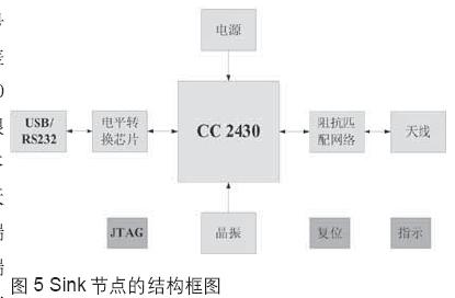
Figure 5 is a structural block diagram of the Sink node we designed. The highly integrated SoC chip CC2430 from Chipcon is still used to implement the data transmission and processing functions of the sensor node. TTL and RS232 level conversion unit uses MAX 3316 chip, which can realize two-channel bidirectional level conversion when power is supplied from 2.25 to 3.0V, and can directly operate the serial data line and control line of CC2430 chip. The peripheral circuit design of CC2430 is the same as the sensor node.
Conclusion
The wireless sensor network based on ZigBee has the obvious advantages of low power consumption, low cost and small size, and can realize the collection, transmission and processing of signals in the monitoring area under a special environment. With the maturity of wireless self-organizing network technology and the introduction of new energy solutions, the application of wireless sensor networks will inevitably spread from military, environmental monitoring, medical care, space exploration and disaster prediction to all areas of life.
LED illuminated neon Open Sign. Energy efficient, 70% less than traditional neon glass tube. Red outline & blue lighted OPEN sign.
Commercial lighted open sign for spa store, massage store, pool, salon, nail store, beach, club, pharmacy store & retail store. Not only a retro neon open sign, but also a decoration sign for window of café, pub, pizza, bakery & cupcake when neon lights up.
Easy installation. Paste adhesive hook (included) on the window, then hang it by hanging chain (included).
Safety, long lifetime & easy operation. Use UL listed LED neon strip & low voltage DC12V adapter (included), a safe guaranty. No battery & remote controller included which will be out of function when cell battery of remote controller is empty (it`s difficult for a common user to replace the cell battery) or keyboard lost.
A unique sign. It`s a handmade crafts by artist. Each Open Neon Light mounted on acrylic board by hands.
Open Sign
Led Open Sign,Open Sign,Open Neon Light,Neon Light Open Sign
Shenzhen Oleda Technology Co.,Ltd , https://www.baiyangsign.com