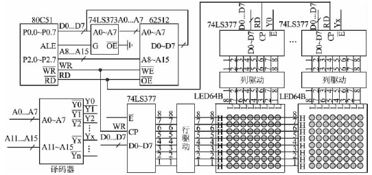
Figure 1 High-speed control scheme LED display electrical principle
There are two characteristics of this solution: First, although the CPU still writes the pattern data of the latch of the column drive circuit through the parallel bus, the latch signal of the latch is changed to the CPU control signal RD instead of the conventional usage WR; Second, the address decoding circuit ensures that the chip select address of the LED dot matrix chip column drive circuit and the logical address of a certain section of the data memory are overlapping, rather than the conventional usage, these two sets of addresses must be separated.
Due to some simple changes in the above circuit, the display control efficiency of the single-chip computer on the LED display screen will change significantly. The specific working process is as follows: Assuming that the data pointer DPTR has been loaded with the address of the data memory, execute the instruction "MOVXA, @DPTR". The function of this instruction is that the CPU reads the font data from the external data memory according to the DPTR and reads it into the accumulator A; but in this circuit, due to the chip select address of the LED dot matrix chip column drive circuit and the data memory The logical addresses of a segment are overlapping, that is to say, when executing the instruction "MOVXA, @DPTR", in addition to pointing to an address in the external data memory, DPTR also selects the latch of a certain LED dot matrix chip drive circuit Device. If the latch pin of the selected latch happens to come in with a pulse, the latch will also lock the font data sent from the external data memory. This pulse is used for RD. RD is the read control signal issued by the CPU to the external data memory when the instruction "MOVXA, @DPTR" is executed. Since the timing of the read control signal RD and the write control signal WR of the MCS51 series of single-chip microcomputers are exactly the same [2], RD replaces WR to achieve the latch function, and of course there is no suspense. When this instruction is executed, it completes the reading of the data memory and also completes the writing of the LED dot matrix, thus speeding up the process of display control.
As mentioned earlier, when the parallel bus is used, the CPU completes the programming process of writing data to the latch of the column drive circuit of the LED dot matrix chip, which takes about ten μs; but now it is only 4 μs, which is much faster, because it is now completed The programming process of writing the mold data to the latch of the column drive circuit of the LED dot matrix once only requires two steps. First, the data pointer DPTR is assigned an effective address, and then the CPU reads the mold data from the external data memory according to the DPTR. At the same time, the font data is also transferred to the latch of the LED dot matrix chip driving circuit. 2 instructions, 4 machine cycles, 4 μs. It is necessary to add a point here, when programming the latch writing data of all LED dot matrix chip drive circuits, do not use cyclic instructions, because then each process has to increase by 2 μs; The method of programming piece by piece, although the program compiled in this way takes up space, but saves time. The design method of using space for time is sometimes a method that designers should try.
The latch control of the row-driven latch of this circuit still uses the write control signal WR of the CPU without change. The chip select signal of the row drive latch also comes from the address decoding circuit. In order to avoid the mutual interference between the data storage and the LED dot matrix, this part of the storage space of the data storage corresponding to this group of addresses is not needed.
The design of the address decoding circuit should ensure that the chip select address of the LED dot matrix chip column drive circuit and the logical address of a certain section of the data memory overlap. Specific design examples are as follows:
Assume that a certain LED display screen uses 240 LED dot matrix chips, which can display 60 Chinese characters of 16 × 16, and a MCS51 series single-chip microcomputer is used for high-speed control. There should be 240 chip select addresses for the 240 LED dot matrix chip column drive circuit. The address decoding circuit must ensure that the effective address after decoding is greater than this number. In the address decoding circuit in FIG. 1, the input address signals are A0 to A7 and A11 to A15, and A8, A9, and A10 are not connected. With the 74LS138 decoder, 256 effective address lines can be obtained after three levels of decoding. The first effective address line corresponds to 8 addresses of the external data memory: 0000H, 0100H, 0200H, 0300H, 0400H, 0500H, 0600H, 0700H. The second effective address line corresponds to the 8 addresses of the external data memory: 0001H, 0101H, 0201H, 0301H, 0401H, 0501H, 0601H, 0701H. ... the 256th effective address line corresponds to the 8 addresses of the external data memory: 00FFH, 01FFH, 02FFH, 03FFH, 04FFH, 05FFH, 06FFH, 07FFH. These 256 effective address lines, 240 chip select addresses for the column drive circuit, and the remaining chip select addresses for the row drive circuit; if not enough, the row drive circuit can be considered to be controlled by a serial bus. The above analysis results show that the I / O interface address of an LED dot matrix chip and the 8-byte address of the data memory establish an overlapping relationship. This is because each LED dot matrix has 8 lines, and each line corresponds to 1 byte of font data.
The above analysis results also show that the mapping relationship is established between the I / O interface addresses of all LED dot matrix chips and the 0000H ~ 07FFH address segment of the data memory. The data memory 0000H ~ 07FFH stores exactly the font data of one frame of image.
Variable Frequency AC Power Supply
Variable Ac Power Supply,Variable Frequency Power Supply,Ac Power Supply Variable Voltage,Ac Power Supply With Variable Frequency
Yangzhou IdealTek Electronics Co., Ltd. , https://www.idealtekpower.com