Much literature and software has been published on the design and the implementaTIon of standard filter responses. When a nonstandard filter response is required, it is often left to the circuit designer to produce a soluTIon using his or her own "standard" set of filter networks . However, there is an alternaTIve to this approach, and it is precise and easy to apply, and it uTIlizes integrator blocks and some simple mathematical manipulation to produce filter responses of any order. The system uses simple op-amp integrator blocks, an example of which is shown in Figure 1, and can equally be applied to both continuous-time and switching-filter (eg, switched-capacitor filter) designs.
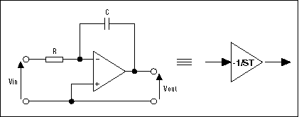
Figure 1. Op-amp-based (linear) integrator circuit block and symbolic representation.
The transfer functions of the integrator in Figure 1 and its symbolic representation are shown in the expression in Figure 2. The response (output) of this circuit to the input voltage is a gain diminishing with frequency at a rate of 6dB per octave with unity gain occurring at a frequency in hertz of 1 / 2Ï€CR.
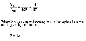
Figure 2. Transfer function of the integrator circuit block in Figure 1.
Application of the TechniqueThe design process starts with the required filter transfer function. The equation in Figure 3, which represents a 2nd-order lowpass-filter response, will be used for illustration purposes, although the technique can be employed for any filter type and is easily extended to higher-order systems.
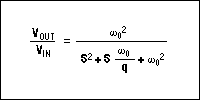
Figure 3. Transfer function of a 2nd-order filter with lowpass response.
A sequence of mathematical steps is then applied to the transfer function to obtain an expression of the form:
VOUT = Æ’ (VIN, VOUT, 1 / S)
Note that all frequency-dependent terms (occurrences of S) in the resulting expression must appear in the denominator terms. This is because the final circuit will be composed of integrators, ie, functions of 1 / S.
Three basic mathematical steps are required. The expression obtained at each stage is given below in the equations of Steps 1 through 3.
Step 1. Cross-multiply to obtain
S² × VOUT + ω / q × S × VOUT + ω0² × VIN
Step 2. Divide by the highest power of S to obtain
VOUT + [(ω0 / q) × VOUT] / S + (ω0² × VOUT) / S = ω0² × VIN / S²
Step 3. Rearrange to obtain an expression for VOUT:
VOUT = VIN × (ω0² / S²)-VOUT × VOUT × (ω0² / S²)-VOUT × [(ω0 / q) / S]
The equation produced in Step 3 is now the defining equation for a network of integrator blocks that will perform the required filtering function.
The remaining two design steps are somewhat intuitive, but the rules are simple. First, an integrator network drawing is produced. This uses a number of integrators and summing nodes to produce a network described by the defining equation. To produce this network, start by Considering the form of the defining equation of Step 3. This expresses the output voltage (VOUT) in terms of functions of VOUT and VIN, where each function is a product of one or more integrator terms.
Considering these terms, from left to right, the first term is a function of VIN and two integrator stages (1 / S²). The signal VIN must therefore pass through two integrator blocks before emerging at VOUT. The first step in producing the diagram is then to draw VIN feeding two integrator blocks in series, with the output of the second integrator connected to VOUT. The second term is also a function of two integrator stages but this time is fed from the VOUT signal. Furthermore, the coefficient of 1 / S² for both of these first two terms is the same, ie, ω 0², so it is reasonable to have the source voltages for both of the first two terms sharing a common path to the output. A summing junction is therefore inserted before the first integrator stage and fed by connections to both VIN and VOUT. The third term of the equation is a function of VOUT and a single integrator stage. To reproduce this in diagrammatic form, VOUT must also be fed to the input of the second integrator block. This is done by inserting a second summing junction, this time before the second integrator block, with inputs taken from the first integrator block and from VOUT.
To complete the network, the correct sign, inverting or noninverting, must be allocated to each summing-junction input. The transfer function of the integrator shown in Figure 1 is of the form -1 / ST, so the integrator blocks will have a signal Inversion built in. Signs are allocated to the summing junctions working from the output back toward the input. The third term in the equation of Step 3 shows that the feedback path from VOUT through the second summing junction and the second integrator and back to VOUT should be inverting. Because the integrator already contains an inversion, the input to the second summing junction from VOUT should be noninverting. By similar analysis, it can be seen that, as the first term of the defining equation is positive, the path from VIN to VOUT should be noninverting. Because both integrators invert the signal, the result is a noninverting path if the inputs to the first and second summing junctions, from VIN and the first integrator block, respectivel y, are each noninverting. Note that this would also apply if both inputs were inverting, but, as we shall see in the final design stage, the natural form of the simple integrator circuit is that of a noninverting summing junction followed by an inverting integrator . The integrator diagram is completed by allocation of a sign to the final summing-junction input, that from VOUT to the first summing junction. This is given by the second term in the defining equation, which is negative. Because the path through both integrators is noninverting, the required inversion must be placed at the input of the signal to the first summing from VOUT. The resulting network for the defining equation of Step 3 is that shown in Figure 4.
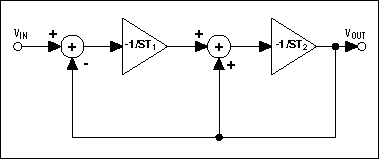
Figure 4. Integrator network representing the defining equation of Step 3.
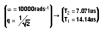
The integrator time constants T1 and T2 can now be assigned. From the integrator network, derivation and analysis of the third term of the defining equation:
-× ω0 / qS = -1 / ST2 → T2 = q / ω0
Similarly, from the first and second terms of the defining equation:
ω0² / S² = 1 / S²T1T2 → T1 = 1 / ω0²T2 = 1 / ωq Values ​​for ω0 and q are then chosen and the time constants T1 and T2 calculated as follows:
The final step is to translate the integrator network of Figure 4 into an operational amplifier / resistor / capacitor circuit. A standard, inverting, op-amp integrator block, comprising an op amp, a feedback capacitor, and an input resistor, is equivalent to a single (noninverting) summing node followed by an (inverting) integrator. Multiple input summing nodes are then accommodated by the addition of more input resistors to the op-amp integrator block.
The circuit in Figure 5 shows the resulting active filter circuit, constructed from op-amp integrator blocks built around the MAX4322. The values ​​given for R1, R2, C1, and C2 produce values ​​for c of 14.96µS and 7.05µS, respectively. The gain response of the filter is shown in the plot of Figure 4.
Note the trick with the feedback to IC1. Strict reproduction of the network in Figure 2 would have required an inverter to be placed in the feedback to the first summing node. Applying feedback directly from VOUT to the noninverting input of IC1 generates a signal at the output of IC1 of (VOUT + VOUT / ST1), which provides the necessary integrating output plus a duplicate of the signal applied from VOUT to the second summing node. Removing the feedback path to the second summing node restores the correct transfer function.
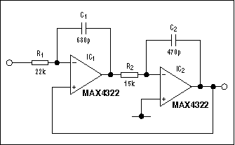
Figure 5. Circuit realization of the integrator network in Figure 2.
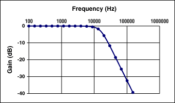
Figure 6. Gain response of the filter in Figure 5.
The above example can be implemented using a simple, dual-op-amp IC and a handful of passive components. Where higher-order systems are being considered, the overall design task can be simplified considerably by the use of multi-stage filter ICs. Two examples of this type of component are the MAX274 and the MAX275. These provide, respectively, 4th-order and 8th-order continuous-time filtering functions based on a series of integrator blocks. The filter time constants for these devices are defined by external resistor values ​​only, as the feedback capacitor for each integrator stage is provided on-chip. If the designer wishes a higher degree of programmability of the filter design, then a switched-capacitor-filter approach may well be suitable. There are a number of switched-capacitor building-block ICs available that can be adjusted by the use of a programmable clock or resistors. Some parts are also available with microprocessor-interface capability. The MAX260 to MAX268 family of swit ched-capacitor-filter building-block parts provide a full range of control methods for anyone looking for programmable filtering functions.
The design process described is powerful in its applicability to virtually any active filtering requirement and can be applied to functions of any order. In addition, the resulting implementation of simple integrator blocks eases the selection and the tolerancing of components. Some active filter implementations exacerbate the effects of basic component tolerances, whereas the integrator approach produces the same basic tolerance susceptibility as that furnished by a passive LCR filter circuit. Further, the effects of op-amp-bandwidth variation are relatively simple to calculate, because the (desired) operating unity -gain bandwidth of each integrator block is simply given by 1 / T rad / s = 1 / 2Ï€RC Hz.
Figure 1. Op-amp-based (linear) integrator circuit block and symbolic representation.
The transfer functions of the integrator in Figure 1 and its symbolic representation are shown in the expression in Figure 2. The response (output) of this circuit to the input voltage is a gain diminishing with frequency at a rate of 6dB per octave with unity gain occurring at a frequency in hertz of 1 / 2Ï€CR.
Figure 2. Transfer function of the integrator circuit block in Figure 1.
Application of the TechniqueThe design process starts with the required filter transfer function. The equation in Figure 3, which represents a 2nd-order lowpass-filter response, will be used for illustration purposes, although the technique can be employed for any filter type and is easily extended to higher-order systems.
Figure 3. Transfer function of a 2nd-order filter with lowpass response.
A sequence of mathematical steps is then applied to the transfer function to obtain an expression of the form:
VOUT = Æ’ (VIN, VOUT, 1 / S)
Note that all frequency-dependent terms (occurrences of S) in the resulting expression must appear in the denominator terms. This is because the final circuit will be composed of integrators, ie, functions of 1 / S.
Three basic mathematical steps are required. The expression obtained at each stage is given below in the equations of Steps 1 through 3.
Step 1. Cross-multiply to obtain
S² × VOUT + ω / q × S × VOUT + ω0² × VIN
Step 2. Divide by the highest power of S to obtain
VOUT + [(ω0 / q) × VOUT] / S + (ω0² × VOUT) / S = ω0² × VIN / S²
Step 3. Rearrange to obtain an expression for VOUT:
VOUT = VIN × (ω0² / S²)-VOUT × VOUT × (ω0² / S²)-VOUT × [(ω0 / q) / S]
The equation produced in Step 3 is now the defining equation for a network of integrator blocks that will perform the required filtering function.
The remaining two design steps are somewhat intuitive, but the rules are simple. First, an integrator network drawing is produced. This uses a number of integrators and summing nodes to produce a network described by the defining equation. To produce this network, start by Considering the form of the defining equation of Step 3. This expresses the output voltage (VOUT) in terms of functions of VOUT and VIN, where each function is a product of one or more integrator terms.
Considering these terms, from left to right, the first term is a function of VIN and two integrator stages (1 / S²). The signal VIN must therefore pass through two integrator blocks before emerging at VOUT. The first step in producing the diagram is then to draw VIN feeding two integrator blocks in series, with the output of the second integrator connected to VOUT. The second term is also a function of two integrator stages but this time is fed from the VOUT signal. Furthermore, the coefficient of 1 / S² for both of these first two terms is the same, ie, ω 0², so it is reasonable to have the source voltages for both of the first two terms sharing a common path to the output. A summing junction is therefore inserted before the first integrator stage and fed by connections to both VIN and VOUT. The third term of the equation is a function of VOUT and a single integrator stage. To reproduce this in diagrammatic form, VOUT must also be fed to the input of the second integrator block. This is done by inserting a second summing junction, this time before the second integrator block, with inputs taken from the first integrator block and from VOUT.
To complete the network, the correct sign, inverting or noninverting, must be allocated to each summing-junction input. The transfer function of the integrator shown in Figure 1 is of the form -1 / ST, so the integrator blocks will have a signal Inversion built in. Signs are allocated to the summing junctions working from the output back toward the input. The third term in the equation of Step 3 shows that the feedback path from VOUT through the second summing junction and the second integrator and back to VOUT should be inverting. Because the integrator already contains an inversion, the input to the second summing junction from VOUT should be noninverting. By similar analysis, it can be seen that, as the first term of the defining equation is positive, the path from VIN to VOUT should be noninverting. Because both integrators invert the signal, the result is a noninverting path if the inputs to the first and second summing junctions, from VIN and the first integrator block, respectivel y, are each noninverting. Note that this would also apply if both inputs were inverting, but, as we shall see in the final design stage, the natural form of the simple integrator circuit is that of a noninverting summing junction followed by an inverting integrator . The integrator diagram is completed by allocation of a sign to the final summing-junction input, that from VOUT to the first summing junction. This is given by the second term in the defining equation, which is negative. Because the path through both integrators is noninverting, the required inversion must be placed at the input of the signal to the first summing from VOUT. The resulting network for the defining equation of Step 3 is that shown in Figure 4.
Figure 4. Integrator network representing the defining equation of Step 3.
The integrator time constants T1 and T2 can now be assigned. From the integrator network, derivation and analysis of the third term of the defining equation:
-× ω0 / qS = -1 / ST2 → T2 = q / ω0
Similarly, from the first and second terms of the defining equation:
ω0² / S² = 1 / S²T1T2 → T1 = 1 / ω0²T2 = 1 / ωq Values ​​for ω0 and q are then chosen and the time constants T1 and T2 calculated as follows:
The final step is to translate the integrator network of Figure 4 into an operational amplifier / resistor / capacitor circuit. A standard, inverting, op-amp integrator block, comprising an op amp, a feedback capacitor, and an input resistor, is equivalent to a single (noninverting) summing node followed by an (inverting) integrator. Multiple input summing nodes are then accommodated by the addition of more input resistors to the op-amp integrator block.
The circuit in Figure 5 shows the resulting active filter circuit, constructed from op-amp integrator blocks built around the MAX4322. The values ​​given for R1, R2, C1, and C2 produce values ​​for c of 14.96µS and 7.05µS, respectively. The gain response of the filter is shown in the plot of Figure 4.
Note the trick with the feedback to IC1. Strict reproduction of the network in Figure 2 would have required an inverter to be placed in the feedback to the first summing node. Applying feedback directly from VOUT to the noninverting input of IC1 generates a signal at the output of IC1 of (VOUT + VOUT / ST1), which provides the necessary integrating output plus a duplicate of the signal applied from VOUT to the second summing node. Removing the feedback path to the second summing node restores the correct transfer function.
Figure 5. Circuit realization of the integrator network in Figure 2.
Figure 6. Gain response of the filter in Figure 5.
The above example can be implemented using a simple, dual-op-amp IC and a handful of passive components. Where higher-order systems are being considered, the overall design task can be simplified considerably by the use of multi-stage filter ICs. Two examples of this type of component are the MAX274 and the MAX275. These provide, respectively, 4th-order and 8th-order continuous-time filtering functions based on a series of integrator blocks. The filter time constants for these devices are defined by external resistor values ​​only, as the feedback capacitor for each integrator stage is provided on-chip. If the designer wishes a higher degree of programmability of the filter design, then a switched-capacitor-filter approach may well be suitable. There are a number of switched-capacitor building-block ICs available that can be adjusted by the use of a programmable clock or resistors. Some parts are also available with microprocessor-interface capability. The MAX260 to MAX268 family of swit ched-capacitor-filter building-block parts provide a full range of control methods for anyone looking for programmable filtering functions.
The design process described is powerful in its applicability to virtually any active filtering requirement and can be applied to functions of any order. In addition, the resulting implementation of simple integrator blocks eases the selection and the tolerancing of components. Some active filter implementations exacerbate the effects of basic component tolerances, whereas the integrator approach produces the same basic tolerance susceptibility as that furnished by a passive LCR filter circuit. Further, the effects of op-amp-bandwidth variation are relatively simple to calculate, because the (desired) operating unity -gain bandwidth of each integrator block is simply given by 1 / T rad / s = 1 / 2Ï€RC Hz.
Digital Accessories producs including Wireless Bluetooth Earphone, Mobile phone Wireless Charger, Mobile phone data cable, Mobile phone selfie holder and Mobile phone USB Disk, etc. They are all computer or mobile phone peripherals products. These kinds of products will bring more convenient when you use mobile phone, they are all real good partners of smart phone. Any inquirey please feel free to contact us and welcome you to visit our company.


Digital Accessories
Digital Accessories,Wireless Charger,USB Data Cable,Bluetooth Selfie Stic
Shenzhen New Wonderful Technology Co., Ltd. , https://www.sznewwonderful.com