MAX2648 5GHz LNA design achieves high frequency stability
Abstract: The RF input-output matching network is a key factor in determining the performance of 5GHz LNA. This application note presents a simple method to ensure that the MAX2648 operates stably at all frequencies by using a capacitive microstrip component in the output matching network. The matching network required for different applications will be slightly different, but the basic principles are suitable for most situations. A small capacitive stub can ensure stability.For more information, wireless product web pages, a quick tour of the MAX2648 data sheet, application technology support, the MAX2648 LNA has a gain of 17dB and a noise figure of 1.8dB in the 5GHz to 6GHz frequency band. Like all excellent microwave devices, the MAX2648 LNA has extremely high gain when operating at high frequencies (up to 20 GHz). As we all know, if appropriate microwave design techniques are not adopted, this amplifier has the potential to self-oscillate at frequencies greater than 10 GHz. This application note describes the design method of the MAX2648 LNA microwave matching circuit to obtain the highest possible performance index while ensuring stable operation. Factors to be considered in the design The following are the factors to be considered when designing a high-performance microwave LNA: Selection of PCB material Selection of power supply bypass input and output matching circuit Selection of PCB material in the 5GHz frequency band, transmission line before and after the low noise amplifier The losses are significant. The line loss at the input of the amplifier is particularly important because this loss will directly add to the noise figure of the LNA. Therefore, it is recommended to use low-loss dielectric materials as PCB materials. For example, the MAX2648 EV kit uses 10mil thick Rogers 4350 "FR4-based laminate" material. The laminated board makes the microwave transmission belt have a stable loss factor, and the FR4 board provides a low-cost support. Capacitor selection In order to achieve the best noise figure, the use of high-Q capacitors in the input and output matching circuit is very important. The use of low-Q components will adversely affect the noise figure. Experiments conducted on the MAX2648 evaluation board show that when ordinary lossy capacitors (such as jelly-bean NPO) are used to replace high-Q capacitors (such as ATC or Vitramon), the noise figure will be lost by 0.2dB. However, high-Q ceramic chip capacitors are too expensive and not suitable for mass product design. As a compromise between cost and performance, Murata's GJ615 series products can be selected. Power supply bypass In order to work stably in the microwave frequency band, power supply bypass is very necessary. It is worth noting that a capacitor with the lowest impedance at the decoupling frequency should be selected. For example, a 1000pF capacitor is not suitable for high-frequency decoupling because its lowest impedance appears below a few hundred MHz. At 5GHz, the self-oscillation frequency will make it more like an inductor. Therefore, when high frequency decoupling, the capacitance should generally be less than 10pF and placed close to the IC. For low frequency decoupling, 1000pF and 0.01µF capacitors are a good choice, and they do not have to be placed directly on the IC pins. Input and output matching The MAX2648 LNA is a high-gain microwave device. In order to work stably at the high-frequency side, it requires suitable input and output matching circuits. Ordinary SMT capacitors and inductors usually have a self-oscillation frequency below 6 GHz. When designing with the MAX2648, care should be taken to avoid using components with a self-oscillation frequency lower than 6 GHz.
To ensure the high frequency stability of the MAX2648, a small capacitive stub should be used as part of the matching circuit at the output. If inductive terminal matching is used at the output of the LNA (especially in series with the coupling capacitor), it will cause high-frequency oscillation, which needs to be avoided in the design. Longer transmission lines will produce inductive effects, it is recommended to use capacitive stubs to compensate for this additional inductance. When the frequency is high and the lumped element exhibits inductive characteristics, the capacitive stub can provide a good capacitance between it and ground. To illustrate this point, compare a circuit simulation with high-frequency oscillations to a circuit simulation without oscillations. It should be noted that the component model used in the simulation will fail when it exceeds its specified frequency. Accurate high-frequency analysis is difficult, but circuit simulation does illustrate its general trend and provides a useful tool for rough estimation of circuit characteristics.
Figure 1 is an ADS simulation curve of an unstable circuit operating around 13.5 GHz. The output matching circuits at this time all use lumped elements. As shown in the schematic below.
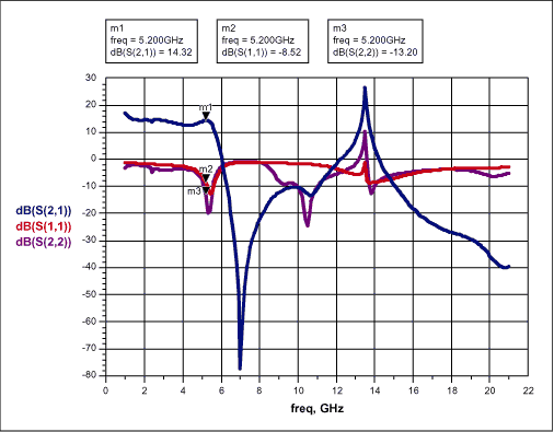
Figure 1. ADS simulation when using lumped components
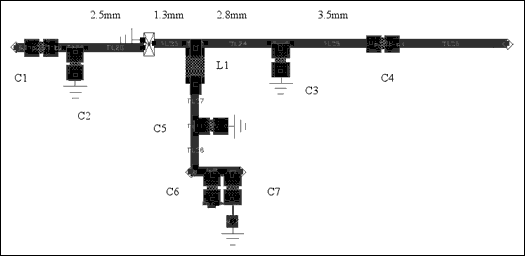
Figure 2. Design drawing of input and output matching circuits (0.4mm line resistance is 50Ω)
| C1 | 2pF |
| C2 | 0.5pF |
| C3 | 0.5pF |
| C4 | 2pF |
| C5 | 1.5pF |
| C6 | 1000pF |
| C7 | 0.01µF |
| L1 | 6.8nH |
Figure 3 shows the results obtained using a capacitive stub, which is achieved by using a wider microstrip line at the output. The electric capacity can be roughly calculated according to the following formula:

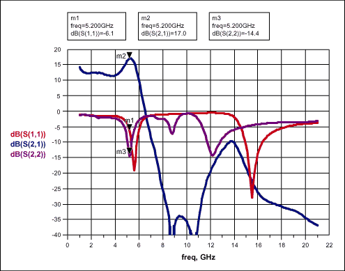
Figure 3. ADS simulation using capacitive stubs at the output
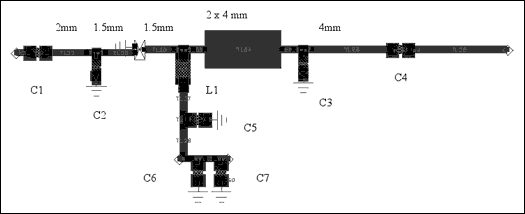
Figure 4. 2mm x 4mm stub wiring diagram (0.4mm lead resistance is 50Ω, the length of the microstrip line is marked on the diagram)
| C1 | 2pF |
| C2 | 0.75pF |
| C3 | 0.5pF |
| C4 | 2pF |
| C5 | 1.5pF |
| C6 | 1000pF |
| C7 | 0.01µF |
| L1 | 6.8nH |
The size of the microstrip line is about 2mm x 3.5mm, the dielectric constant is 4.1, the substrate thickness is 0.2mm, and the capacitance is about 1.27pF, ignoring the edge effect. To facilitate tuning, a capacitor is connected in parallel with ground. Adjust the position of the input and output bypass capacitors as necessary to obtain the best noise figure and gain. Summary The input and output matching network is a key factor in determining the performance of low-noise amplifiers. This application note gives a simple way to ensure that the MAX2648 works stably at all frequencies, that is, using a capacitive microstrip line in the output matching network. Different applications require slightly different matching networks, but the basic principles are suitable for most situations.
Spiral Candle usually six colors , 22Gram Spiral Candle is the popular in Jeddah . every month we ship Spiral Taper Candle to Jeddah . we are about customer . so early receive deposit and ship fastly. Birthday Spiral Candles usually be used for party ,dinner ,festival . 22G Colorful Spiral Candle 's package details is each pcs WRAPPED BY CELLOPHANE,12PCS(2pc*6colors)IN ONE BLUE BOX AND box with SHRINK PACKED,24BOXES/CARTON. 22g Spiral Taper Candle can be loaded about 2200catons . we will try our best to load full .
Welcome to new and old customer order !
22Gram Spiral Candle,22G Colorful Spiral Candle,Birthday Spiral Candles,Spiral Taper Candle
Shijiazhuang Zhongya Candle Co,. Ltd. , https://www.zycandlefactory.com