Achieving high-speed, large-capacity storage of data is a key technology in data acquisition systems. This design uses ALTEra's Cyclone series FPGA to complete the control of DDR SDRAM, describes the various timing operations of DDR SDRAM with state machine, and designs the data and command interface of DDR SDRAM. The control core is used to simplify the operation of the DDR SDRAM, and the top-down modular design method is adopted to embed the control core into the control module of the entire data acquisition system, thereby completing high-speed data acquisition, storage and uploading. The controller's workflow was verified and debugged using the logic analyzer SignalTap II embedded in the development software QUARTus II. The resulting data waveform shows that the burst read and write operations to the DDR SDRAM have been completed, achieving the desired design goals.
DDR SDRAM is the abbreviation of Double Data Rate SDRAM, which is double rate synchronous dynamic random access memory.
DDR memory is developed on the basis of SDRAM memory. It can transfer data once on the rising and falling edges of the clock, and achieve higher data transfer rate at the same bus clock frequency as SDRAM. In this design, Altera's Cyclone series model EP1C6Q240C8 FPGA implementation controller is used. The HY5DU121622B(L)TP DDR SDRAM produced by Hynix is ​​used as the memory to complete high-speed and large-capacity storage of data.
1 DDR SDRAM control principle and storage function realization
There are 7 common commands supported by DDR SDRAM: No Operation, Active, BurstRead, Burst Write, Autorefresh, Precharge, Mode. Register Register (Mode Register Set). All operation commands are realized by common control of the signal lines RAS_N, CAS_N, and WE_N. Before accessing the DDR SDRAM, first initialize it, that is, set the normal mode register and extended mode register of the DDR SDRAM to determine the working mode of the DDR SDRAM. These settings include burst length, burst type, and CAS latency. And the operating mode and the setting of the enable and output drive capability of the DDR SDRAM internal delay locked loop (DLL) in the extended mode register.
After the initialization is completed, the DDR SDRAM enters the normal working state, and the memory can be read, written, and refreshed. DDR SDRAM operates under the control of a pair of differential clocks. Commands (address and control signals) are triggered on the rising edge of each clock. Along with the data DQ, a bidirectional data strobe signal DQS is also included, through which the receiver receives data. The DQS is generated as a strobe signal by the DDR SDRAM during the read cycle and by the controller of the memory during the write cycle. The strobe signal is related to the data and acts like an independent clock and meets the corresponding timing requirements. Since the data interface of the DDR SDRAM operates under the triggering of both edges of the clock, its data width is half the width of the memory data. In order to realize large-capacity storage of data, a control core is used to operate two DDR SDRAMs at the same time, and the width of the external data line is extended from 16 bits to 32 bits of the single-chip DDR SDRAM.
The read and write operations to the DDR SDRAM are burst based, that is, starting from a selected address unit, successively accessing the address unit of the set length, the length is the so-called burst length. The programmable read or write burst length provided by DDR SDRAM is 2, 4 or 8. Data access begins with an active command (Active) followed by a read (BurstRead) or write (Burst Write) command. The address bits that are triggered along with the activation command are used to select the region and page (or row) to be accessed, and the address bits that are triggered along with the read or write command are used to select the starting column unit for the burst access. After the read command is triggered, the data will appear on the data bus after 1.5 to 3 clock cycles. This delay is the so-called CAS latency, the time it takes to read data from the DDR SDRAM core until the data appears on the data bus. The size of the CAS latency is related to the speed of the SDRAM and the clock frequency of the memory. When accessing a different row of address units, the current line needs to be closed by a precharge operation.
The Autorefresh command is used to periodically refresh the DDR SDRAM to keep its internal data from being lost. 2 DDR SDRAM Controller Design The features of the DDR SDRAM controller include:
(1) Initializing DDR SDRAM;
(2) Simplify the read and write timing of DDR SDRAM;
(3) Converting the dual clock edge data of the DDR SDRAM interface into single clock edge data, so that the operation of the DDR SDRAM is similar to the ordinary RAM;
(4) The controller also generates periodic refresh commands to maintain data in the DDR SDRAM without loss. Its control conversion diagram is shown in Figure 1.
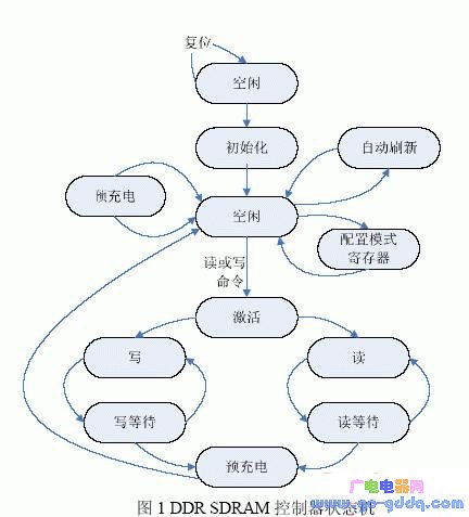
After the initialization of the DDR SDRAM is completed, it can be read, written or otherwise manipulated. Before executing a read (write) command, the row to be read (written) is activated, and then the row can be read (written). In the design of the controller, all read and write commands are not pre-charged. Therefore, after a row is activated, it will remain active until the user sends a burst termination command, and the controller will automatically generate a pre- Charge the command to close the current line. In this way, after a row is activated, the user can perform continuous burst read (write) operations, thereby saving the activation time required for each burst read and write, and improving the data throughput rate of the system.
Pharmaceuticals,2-Methyl- Propanoic Acid Monohydrate Price,2-Methyl- Propanoic Acid Monohydrate Free Sample,Pure 2-Methyl- Propanoic Acid Monohydrate
Zhejiang Wild Wind Pharmaceutical Co., Ltd. , https://www.wild-windchem.com