1 Introduction
Compared with traditional light sources such as incandescent lamps and fluorescent lamps, high-power white LED solid-state light sources have the advantages of energy saving and environmental protection. Now the highest level of white light LED light efficiency has reached 70lm / W, under the condition that the chip size is kept 1mm × 1mm, as the LED power increases, the heat flux density of the LED chip to the heat sink increases, if the heat dissipation is not solved Well, the heat inside the chip gathers, and the junction temperature rises continuously, which causes a series of problems such as drift of the emission wavelength, decrease of the light extraction efficiency, accelerated aging of the phosphor, and shortened service life. Thermal resistance is the main parameter to measure the heat dissipation of high-power LEDs. There are significant differences in the thermal resistance of devices with different structures and bonding processes.
Determining the thermal resistance first measures the junction temperature of the device. Since the heat generating layer of the compound semiconductor device is usually a quantum well active region of the order of nm inside thereof, temperature measurement is difficult. The micro-coupler contact measurement method can only touch the surface of the chip electrode or the light-emitting surface, and the average temperature of the surface of the chip exposed to the air and directly contact with the thermocouple is obtained, and the LED that has packaged the phosphor and the lens cannot be measured. . Infrared imaging method, because the thermal infrared information of different layers of the chip interfere with each other to form noise, and can not accurately sense the internal active layer temperature, which is also more difficult to measure for the packaged white light device.
In this paper, the measurement system developed by the principle of forward voltage method realizes the accurate measurement of high-power LED junction temperature, which has great reference value for improving the heat dissipation characteristics and life evaluation of high-power LED. At the same time, the system is used to compare the thermal resistance of high-power LEDs with different chip structures and different packaging processes, and the high-power LED luminescence characteristics under different junction temperatures are measured and compared.
2 Measurement principle and device
2.1 The principle and measurement process of measuring junction temperature by forward voltage method
Under a certain injection current I, the forward working voltage Vf of the LED can be expressed as

Where: Vfjunction is the junction voltage of the PN junction; Rconductor is the resistance of each material in the injection current path; Rcontact is the contact resistance between different materials in the current path.
From the most basic Shockby equation, the relationship between the junction voltage Vfjunction and the junction temperature T is
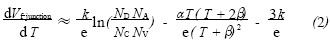
Where: k is the Boltzmann constant; e is the electron energy; ND is the donor impurity concentration; NA is the acceptor impurity concentration; NC is the state density of the conduction band bottom; NV is the state density of the valence band top; α, β is Two normal numbers in the relationship between the semiconductor band gap and temperature. Compound semiconductor devices generally operate in a strong ionization interval where the carrier concentration ni generated by the intrinsic excitation is much smaller than the ion concentration of the donor acceptor impurity. It can be considered that ND and NA do not substantially change with temperature, and the relationship between NC and NV and junction temperature is

Where: mn is the density of the states of electrons and mp is the effective mass of the density of holes. It can be seen from the formula (3) that the first term in the formula (2) is a negative value. In the formula (2), α and β are two normal numbers, which are related to the material. Therefore, the derivative of the junction voltage in equation (2) versus the junction temperature is a negative constant, which is related to the semiconductor material and doping. For the GaN material, α = 0.77 meV/K2, β = 600 K, and if the doping concentration of the donor and acceptor impurities is NA = ND = 2 × 10 16 cm 3 , the temperature coefficient of the junction voltage Vfjunction can be calculated to be 1.74 mV/K. It can be seen from equation (1) that the forward voltage includes not only the junction voltage Vfjunction, but also the resistance Rconductor of each body material in the current path and the contact resistance Rcontact between different materials. These factors also vary with temperature, and the temperature is constant. The voltage relationship has a certain contribution. Under different chip structures, the composition and contact conditions of Rconductor and Rcontact are different, and the temperature and voltage coefficient K may be different.
Experiments show that the forward voltage of most semiconductor devices has a good linear relationship with the junction temperature when the input current is constant. It is only necessary to measure the voltage at a junction temperature, according to the linear relationship and a certain junction temperature and voltage base point. The exact value of the junction temperature is determined, so the temperature voltage coefficient K is first measured. Select static calibration at a small current (requires that this current does not have a large effect on the junction temperature, usually less than 1% of the normal operating current), obtain the K value under small current conditions, and then dynamically measure the power LED device at The trend of the instantaneous forward voltage of the large current to the small scale current is converted, and the accurate value of the junction temperature is obtained.
The measurement process is:
1) Calibration. This is the key to quantitative measurement of junction temperature, in order to obtain the temperature and voltage characteristics of various devices. After the calibration current Is is selected, the PN junction of the device is kept in a different constant temperature field, and the forward voltage of the device at different junction temperatures is measured, and K is fitted.
2) Dynamic measurement. The LED is energized and kept in the working state, and the junction temperature when the heat balance is reached is the junction temperature under the working state to be tested. The power is turned off to make the LED out of the working state, and the calibration current is turned on at the same time. The forward voltage rises exponentially with time. The high-speed precision sampling measures the change of the forward voltage of the LED during the cooling process, and obtains the dynamic curve of the junction temperature.
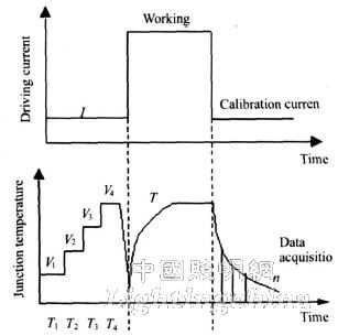
Figure 1 Forward voltage method for measuring LED junction temperature
3) Data processing. The exponential change trend of the voltage with time is analyzed to find the forward voltage of the LED at the time of power-off, and the accurate value of the junction temperature is calculated by the linear relationship. According to the junction temperature, the heating power and the temperature of the corresponding heat sink location, the thermal resistance from the junction to the heat sink location can be calculated.
2.2 Measuring device
Self-developed junction temperature test system based on forward voltage method can obtain K of different chips, can accurately measure junction temperature of LED working state under different ambient temperature and different working current, and the junction temperature measurement accuracy reaches ±0.5 °C, and according to the knot The temperature calculates the thermal resistance of the active area of ​​the chip to the heat sink, and at the same time, it can measure the change rule of the LED junction temperature during the whole dynamic process of the LED from the working state to the steady state. This system is capable of measuring junction temperature and thermal resistance of a compound semiconductor device having a PN junction structure.
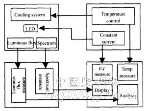
Figure 2 Measurement system block diagram