Successive approximation, analog-to-digital converter (SAR-ADC) is simple and straightforward. The user connects the analog voltage to the input (AINP, AINN, REF) and sees an output digital code that represents the analog input relative to the reference. Voltage.
At this point, the user may want to analyze the converter's specifications to verify that the converter's operation meets the standards in the datasheet. Especially when the user finds that it is not fast enough, it is more necessary to determine whether the converter has received the correct internal analog signal.
Users can use simulation tools to predict the likelihood of these problems and solve them. The determination of the ADC analog input stage simulation depends on the accuracy of the voltage and current. It is in this respect that the simulated SPICE macro model works. PCB digital signal integrity depends on timing, voltage-current levels, and parasitic effects. The digital IBIS model will be useful in this regard. We will talk about IBIS next month, but let us first solve the ADC simulation environment.
SPICE simulation for ADC
The trial and error method of transmitting signals to the ADC is time consuming and does not necessarily work. If the user's analog input pin is unstable at a critical point in time when the converter is capturing voltage information, it is unlikely that the correct output data will be obtained. The first step in the SPICE model that allows you to do this is to verify all of the analog inputs so that no error signals get into your converter.
Let's take a closer look at a typical serial, pseudo differential SAR-ADC device similar to the ADS8860 (Figure 1).
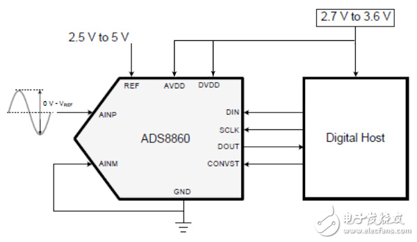
Figure 1 The ADS8860 is a pseudo differential input, 1MHz, 16-bit SAR-ADC.
The device's TINA-TI SPICE model allows the user to simulate the effects of analog signals entering the converter. With this model, and the appropriate driver op amp model on AINP, AINM, and REF, determine if a good conversion can be achieved before the user performs the actual PCB operation. The importance of the ADC macro model is that it accurately describes the characteristics of the converter's input terminals. Op amps that drive AINP, AINN, and REF must also accurately simulate their open-loop output resistance (Ro).
Let's take a closer look at how this macro model works. This converter macro model uses a 55pF sampling capacitor to sample the positive and negative inputs separately. This device converts the voltage difference between the two sampled values ​​on AINP and AINN. As shown in the simulation results, this model must be stable to at least half of a least significant bit (LSB) at the end of the acquisition cycle. For this 16-bit converter, half of an LSB is equal to REF / 216.
The voltage reference pin, REF, needs to be stable during the conversion process or before the CONVST pin goes high (Figure 2). When CONVST is low, the converter is acquiring an input signal (acquisition mode). The SAR-ADC macro model has a 1 MHz clock and does generate a CONVST signal. At the end of the bit conversion period, the voltage reference pin must be stable at half the LSB level throughout the converter's conversion time.

Figure 2 shows the role of CONVST in chip selection in this three-line development diagram that supports three-wire operation.
The TINA-TI model for the ADS8860 in Figure 3 samples the input signals on AINP and AINN and gives the sampled results on the model's AINPsmpl and AINMsmpl.
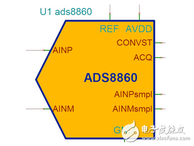
The top graph in Figure 3 shows the TINA-TI macro model of the SAR-ADC.
In Figure 4, the input on AINP is equal to 3V and the reference voltage is equal to 4.096V. When the user tests the accuracy of the input signal, the ADS8860 TINA-TI circuit is set to the difference between the sense amplifier driver, the output of AMP_OUT_sig, and its output signal, AINPsmpl. When observing this difference, check the end of the sampling time, or the area just before the CONVST pin goes high. Verify that this signal is less than half of the LSB.
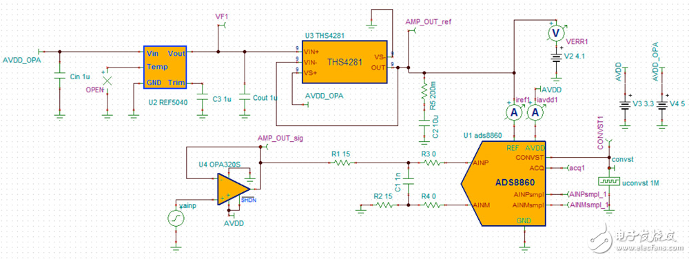
Figure 4 This setup is used for TINA-TI circuit monitoring analog and reference inputs.
Once the user has checked the analog input function for accuracy, then the stability of the voltage reference pin needs to be checked. The voltage difference between the voltage reference output (VF1) and the THS4281 amplifier output (AMP_OUT_ref) is measured when the user measures the accuracy of the REF pin. Be sure to use the value of VERR1 to remove the offset error generated by the voltage reference (REF5040) and the op amp (THS4281). While doing these operations, use the iref1 ammeter to check the voltage level just before the current peak appears.
in conclusion
The simulation for SAR-ADC is more complicated. For now, there is no complete converter model that accurately models the entire device. The existing resource is a simulated SPICE file that simulates the stability of the input pin. With it, users have a powerful tool that allows users to solve one of the most critical and toughest converter problems.
However, this is not enough. You only simulated the analog components of the ADC. We will talk about how to simulate the digital input/output of the converter next month.
High-power Led Street Lamp is a kind of mainstream light source configuration widely used in Road Lighting project.The aluminum alloy surface of its radiator is treated with deep anodic oxidation, which can resist all kinds of harsh environment.In addition, its patented vertical natural convection heat dissipation structure, high heat dissipation efficiency, small volume, light weight, at the same time, it uses high quality long life LED packaging materials, LED light pass maintenance rate.

Technical parameters
|
Power source |
AC85~260V/50~60Hz |
|
Power |
60W-120W |
|
LED junction temperature |
<60℃ |
|
LED luminous efficiency |
>100 Im/W |
|
The initial light flux |
6000Lm-12000Lm |
|
Light output efficiency of light |
>90% |
|
Color temperature |
4000K-6500K |
|
Color rendering |
Ra>75 |
|
Power factor |
>0.95 |
|
Protection class |
IP65 |
|
Operating temperature |
-40℃~+50℃ |
|
Wind Index |
12 level |
|
Lamp life |
>50000h |
High Power Led Street Lamp,Led Street Lamp,Led Street Lamp Bulbs,Led Street Lamp Price
Jiangsu chengxu Electric Group Co., Ltd , https://www.satislighting.com