On this basis, the digital energy spectrum measurement experimental device was established through circuit design. The energy spectrum of 137Cs was measured. The measurement results were in good agreement with the measured spectrum of the simulated energy spectrometer under the same conditions. This proves that the hardware design scheme of digital multi-channel pulse amplitude analyzer based on FPGA is correct and feasible, and has practicality.
0 Preface
Multichannel pulse amplitude analyzers and ray energy spectrometers are commonly used in nuclear monitoring and technology applications. In the 1990s, a new multi-channel spectrometer based on high-speed nuclear pulse waveform sampling and digital filter forming technology was introduced abroad, which made digitalization an important direction for the development of pulse energy spectrometer. Domestic spectrometer technology has been stuck at the level of analog technology for many years, and digital energy spectrum measurement technology is still in the method research stage. In order to meet the growing demand for high performance spectrometers, there is an urgent need to develop a digital gamma spectrometer. The nuclear energy spectrum displayed on the display by a nuclear pulse analyzer helps people understand the extent of radioactivity from nuclear matter.
1 Advantages of digital multichannel analyzer
A large number of scholars in China use the nuclear spectrometer analog circuit to realize the processing of pulse accumulation. Since the whole process is realized by analog circuits, it has been plagued by various unfavorable factors: the limited processing capability of the analog filter shaping circuit does not meet the requirements of optimal filtering; the energy resolution of the analog system is significant at high count rates. Decline, low pulse pass rate; inherent temperature drift and difficult adjustment of the analog circuit, resulting in system stability, linearity and low adaptability to different applications; more complex applications such as pulse waveform recognition, charge trapping effect correction, etc. The occasional simulation system is not up to the task.
In comparison, the performance of the digital pulse amplitude analysis system is significantly better than the analog pulse analyzer. The digital analyzer has the following advantages: it realizes the stability and reliability of the system through software implementation; it can use the digital signal processing method to achieve optimal design for the input noise characteristics to achieve the best or quasi-optimal filtering effect; The anti-stacking ability is strong, and the pulse passing rate is higher under the same energy resolution; the parameters are controlled by the program, and the adjustment is convenient and simple.
2 overall design
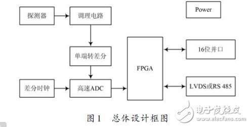
This scheme designs a hardware platform based on programmable gate array multi-channel pulse amplitude analyzer. Figure 1 is the overall design block diagram. The nuclear pulse signal output by the detector is simply conditioned by the front-end circuit. After single-ended to differential, the high-speed ADC with a sampling rate of 65 MHz is subjected to analog-to-digital conversion under the control of the FPGA to complete the core. The digitization of the pulse and the formation of a nuclear energy spectrum in the FPGA by the digital nuclear pulse processing algorithm can be transmitted to other spectral data processing terminals through a 16-bit parallel interface, or remotely transmitted through the LVDS/RS 485 interface. It is important to note that due to the high-speed AD pre-position, the conditioning circuit should meet the requirements of wideband, high speed, and dynamic adjustment of circuit parameters to adapt to the signals output by different types of detectors, so as to better utilize the advantages of digital technology.
3 specific hardware design
3.1 front end circuit
The front end circuit consists of a single-ended to differential and high speed ADC circuit. Differential circuits are widely used due to their good resistance to common mode interference. Since the pulse signal output from the conditioning circuit is a unipolar signal, if it is directly sent to the ADC, half of the dynamic range will be lost. In the design, an appropriate bias voltage is added to the op amp to convert the unipolar signal into a bipolar signal and then sent to the ADC to ensure the dynamic range. While converting the signal from single-ended to differential, anti-aliasing filtering is performed to complete the bandwidth adjustment.
This design uses the AD9649-65 high-speed ADC to achieve analog-to-digital conversion of the core pulse. The AD9649 is a 14-bit parallel output high-speed analog-to-digital converter with low power consumption, small size, and good dynamic characteristics. When the signal passes through the conditioning circuit and passes through the differential circuit to the single-ended circuit, it enters the ADC as a differential signal. Under the control of the differential clock, it is converted into 14-bit data and enters the FPGA. The high-speed A/D is in the external FPGA. The signal is sampled under control. The sampled digital signal is then sent to the FPGA for amplitude extraction of the digital core pulse. Figure 2 shows the schematic of the A/D conversion. The AD9649 performs A/D conversion under the synchronization of the differential clock. D0~D13 are 14 valid output data bits.
![On this basis, the digital energy spectrum measurement experimental device was established through circuit design. The energy spectrum of 137Cs was measured. The measurement results were in good agreement with the measured spectrum of the simulated energy spectrometer under the same conditions. This proves that the hardware design scheme of digital multi-channel pulse amplitude analyzer based on FPGA is correct and feasible, and has practicality. 0 Introduction Multichannel pulse amplitude analyzers and ray energy spectrometers are commonly used in nuclear monitoring and technology applications. In the 1990s, a new multi-channel spectrometer based on high-speed nuclear pulse waveform sampling and digital filter forming technology was introduced abroad, which made digitalization an important direction for the development of pulse energy spectrometer. Domestic spectrometer technology has been stuck at the level of analog technology for many years, and digital energy spectrum measurement technology is still in the method research stage. In order to meet the growing demand for high performance spectrometers, there is an urgent need to develop a digital gamma spectrometer. The nuclear energy spectrum displayed on the display by a nuclear pulse analyzer helps people understand the extent of radioactivity from nuclear matter. 1 Advantages of digital multi-channel analyzer A large number of scholars in China use the nuclear spectrometer analog circuit to realize the processing of pulse accumulation. Since the whole process is realized by analog circuits, it has been plagued by various unfavorable factors: the limited processing capability of the analog filter shaping circuit does not meet the requirements of optimal filtering; the energy resolution of the analog system is significant at high count rates. Decline, low pulse pass rate; inherent temperature drift and difficult adjustment of the analog circuit, resulting in system stability, linearity and low adaptability to different applications; more complex applications such as pulse waveform recognition, charge trapping effect correction, etc. The occasional simulation system is not up to the task. In comparison, the performance of the digital pulse amplitude analysis system is significantly better than the analog pulse analyzer. The digital analyzer has the following advantages: it realizes the stability and reliability of the system through software implementation; it can use the digital signal processing method to achieve optimal design for the input noise characteristics to achieve the best or quasi-optimal filtering effect; The anti-stacking ability is strong, and the pulse passing rate is higher under the same energy resolution; the parameters are controlled by the program, and the adjustment is convenient and simple. 2 Overall design This scheme designs a hardware platform based on programmable gate array multi-channel pulse amplitude analyzer. Figure 1 is the overall design block diagram. The nuclear pulse signal output by the detector is simply conditioned by the front-end circuit. After single-ended to differential, the high-speed ADC with a sampling rate of 65 MHz is subjected to analog-to-digital conversion under the control of the FPGA to complete the core. The digitization of the pulse and the formation of a nuclear energy spectrum in the FPGA by the digital nuclear pulse processing algorithm can be transmitted to other spectral data processing terminals through a 16-bit parallel interface, or remotely transmitted through the LVDS/RS 485 interface. It is important to note that due to the high-speed AD pre-position, the conditioning circuit should meet the needs of wideband, high speed, and dynamic adjustment of circuit parameters to adapt to the signals output by different types of detectors, so as to better utilize the advantages of digital technology. 3 Specific hardware design 3.1 Front-end circuit The front-end circuit consists of a single-ended to differential and high-speed ADC circuit. Differential circuits are widely used due to their good resistance to common mode interference. Since the pulse signal output from the conditioning circuit is a unipolar signal, if it is directly sent to the ADC, half of the dynamic range will be lost. In the design, an appropriate bias voltage is added to the op amp to convert the unipolar signal into a bipolar signal and then sent to the ADC to ensure dynamic range. While converting the signal from single-ended to differential, anti-aliasing filtering is performed to complete the bandwidth adjustment. This design uses the AD9649-65 high-speed ADC to achieve analog-to-digital conversion of the core pulse. The AD9649 is a 14-bit parallel output high-speed analog-to-digital converter with low power consumption, small size, and good dynamic characteristics. When the signal passes through the conditioning circuit and passes through the differential circuit to the single-ended circuit, it enters the ADC as a differential signal. Under the control of the differential clock, it is converted into 14-bit data and enters the FPGA. The high-speed A/D is in the external FPGA. The signal is sampled under control. The sampled digital signal is then sent to the FPGA for amplitude extraction of the digital core pulse. Figure 2 shows the schematic of the A/D conversion. The AD9649 performs A/D conversion under the synchronization of the differential clock. D0~D13 are 14 valid output data bits. 3.2 FPGA At present, there are two main schemes for digital realization of multi-channel pulse amplitude analysis at home and abroad: pure DSP scheme and DSP+ programmable device scheme. This paper will give full play to the parallel processing advantages of FPGA, realize the nuclear pulse acquisition and digital nuclear pulse processing algorithm on a single FPGA chip. After quar-tus-II software simulation and synthesis, this paper selects EP3C40 FPGA chip to realize multi-channel analyzer. Digital features. 3.3 Interface Circuit Design The interface circuit design uses two long-distance data transmission interfaces, LVDS and RS485, for remote transmission of nuclear energy spectrum data. LVDS is a low-voltage differential signal that is a point-to-point or point-to-multipoint connection with low power consumption, low bit error rate, low crosstalk, low noise and low radiation. LVDS is becoming more and more widely used in systems that require high signal integrity, ground jitter, and common mode. Figure 3 shows the LVDS interface circuit with a low voltage and a maximum data transfer rate of 655 Mb/s. In the high-speed communication state, the communication distance can reach several hundred meters. The RS 485 interface uses a combination of balanced drivers and differential receivers, and has strong anti-common-mode interference and noise immunity. The maximum communication distance is about 1 219 m, and the maximum transmission speed is 10 Mb/s. The transmission rate is inversely proportional to the transmission distance. At a transmission rate below 100 Kb/s, the maximum communication distance can be achieved. 3.4 Power Circuits There are two main types of regulated power supplies: linear regulated power supplies and switching regulated power supplies. The power-regulating switching transistor of the switching power supply works in the switching state, which is prone to serious switching interference. If the switching power supply is used, these interferences will seriously affect the normal operation of the digital multi-channel analyzer and reduce the A/D conversion accuracy. Therefore, this article uses a linear regulated power supply to power each functional module. The advantage of the linear regulated power supply is that the output voltage is lower than the input voltage, the reaction speed is fast, the output ripple is small, and the noise generated by the operation is low. The power supply circuit designed in this paper has an input voltage of 9~12 V, and the output voltage is 5 V, 3.3 V, 2.5 V, 1.8 V, and 1.2 V. The linear regulator circuit is single-ended to differential, ADC, FPGA, LVDS and other modules. powered by. 4 Digital peaking NaI (Tl) detector output signal through the conditioning circuit into the high-speed ADC, the ADC for continuous high-speed sampling, and then the FPGA completes the digital nuclear pulse signal integration, peak detection, threshold judgment and other functions [8]. Since the first derivative of the nuclear energy spectrum is 0 when the nuclear energy spectrum reaches a peak, the peak of each nuclear pulse can be found in the continuous input signal, and the peak value of the corresponding channel address is increased by 1, thereby forming a nuclear energy spectrum. In order to improve the peak-financing efficiency, the threshold value of the discrete pulse signal needs to be judged before the peak finding, and the peak-level processing is not performed on the signal whose amplitude is lower than the lower threshold, which can greatly reduce the discrete nuclear pulse signal participating in the peak finding. 5 Functional Testing The spectral data processing PC software was developed using the Borland C++ integrated development environment. The software implements functions such as spectrum display, spectrum data management, system parameter setting, and RS 485 communication. Figure 4 shows the 1 024 energy spectrum obtained by the digital multi-channel analyzer designed by the digital multi-channel analyzer. The energy resolution is close to 8%. 6 Conclusion This paper presents an FPGA-based digital nuclear pulse analyzer hardware design. The scheme realizes the multi-channel pulse amplitude digital analysis function in a single-chip FPGA. Through the software function simulation and actual operation, the feasibility of the hardware design of the digital multi-channel pulse amplitude analyzer is demonstrated, and the FPGA is applied to the digital energy spectrum measurement system. Can fully utilize its parallel processing advantages, and can effectively reduce the complexity of hardware circuit design. (Author: Cui Chen Yuan, has Weihua, Chen, Xu Austria)](http://i.bosscdn.com/blog/15/40/32/4-131121111951N6.jpg)
Yaxing provides very thin thickness and special compound skived tapes from 0.03mm to 2.0mm, whose excellent and stable quality only the most advanced technologies, the most selected raw materials and skilful experts could granted.
PTFE Film,White PTFE Film ,Black PTFE Film,Yellow PTFE Film
TAIZHOU YAXING PLASTIC INDUSTRY CO., LTD , https://www.yaxingptfe.com