How to make electronic fake load

The electronic dummy load serves as a modern alternative to traditional load resistance boxes and sliding line varistors, particularly excelling in scenarios where constant current or constant voltage settings are required—something conventional varistors cannot easily achieve. It is widely used for testing the output characteristics of various power devices such as generators, AC/DC and DC/DC converters, uninterruptible power supplies (UPS), dry batteries, batteries, transformers, and chargers. This device can handle a maximum dummy load power of up to 600W, with adjustable resistance ranging from 30mΩ to 14.352kΩ, offering high flexibility and precision. **First, the basic idea** When designing an electronic dummy load, it's common to use FETs or IGBTs because they require low control power. However, it’s crucial to ensure that these components have sufficient power margin at full load to prevent damage during operation. Since the dummy load generates a significant amount of heat, a proper heat sink must be used, and the thermal resistance between the power device and the heat sink should be minimized. In some cases, a cooling fan may also be necessary. Another critical consideration is the risk of parasitic self-oscillation in power devices, which can cause instability and even lead to component failure. Therefore, anti-parasitic oscillation measures are essential for the successful design of an electronic dummy load. The circuit typically starts by generating a reference voltage that is sent to three operational amplifiers. These op-amps help implement the core functions of the dummy load: constant voltage and constant current. A general principle block diagram is shown in Figure 1.

How to make electronic fake load

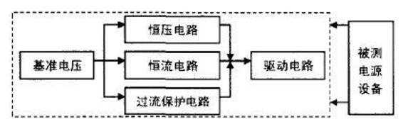
Figure 1: Block Diagram

**Second, the circuit principle** The schematic is illustrated in Figure 2. The main circuit, excluding the dotted-line frame 5 and the two multimeters, includes a constant voltage circuit, a constant current circuit, an overcurrent protection circuit, and a drive circuit. The input voltage is 12V, which passes through a current-limiting resistor R1 to the cathode K of the three-terminal adjustable shunt reference source U1 (TL431). The reference voltage VR from the reference terminal R is 2.5V, and this value is adjusted using a variable resistor R6 connected through R1. One path provides voltage for U3A via R2, while another path supplies voltage for U3C through R7.

How to make electronic fake load

**1. Constant Voltage Circuit** As shown in Figure 2, when the input voltage increases, the non-inverting input voltage of U3A rises. If this voltage exceeds the inverting input (reference voltage), U3A outputs a high level, reducing the gate voltage (VG) of the field-effect transistors Q1–Q4. This causes the drain-source voltage (VDS) to drop, maintaining a stable output voltage. **2. Constant Current Circuit** In this mode, as the load current increases, the voltage across resistors R19, R22, R25, and R28 also rises. This increases the sampling voltage on R18, R21, R24, and R27, raising the inverting input voltage of U3C. When this voltage surpasses the non-inverting input, U3C outputs a low level, lowering the gate voltage of the FETs and increasing their internal resistance (RDS), thus limiting the load current and maintaining a constant value. **3. Overcurrent Protection Circuit** If the load current continues to rise, the voltage at the inverting input of U3B increases. Once it exceeds the preset overcurrent threshold, U3B outputs a low signal, reducing the gate voltage of the FETs and increasing their RDS. This effectively limits the current and protects the circuit from overloads. **4. Drive Circuit** The drive circuit uses high-power FETs like IRF540 as the main power components. However, connecting multiple FETs in parallel can increase inter-electrode capacitance and distributed capacitance, leading to frequency-induced parasitic oscillations. To mitigate this, each transistor is connected with a series resistor (R17, R20, R23, R26) to suppress oscillation. Resistors R18, R21, R24, and R27 are used for voltage sampling, while R19, R22, R25, and R28 act as current limiters. A capacitor (C9) is connected between the drain of the FET and ground to reduce vibration. **Third, the circuit test** After building the dummy load, testing is essential. The test setup is shown in Figure 2, including the dotted box 5 and two multimeters. Multimeter 1 measures the output voltage, and multimeter 2 measures the output current. Both potentiometers are set to 50%. When the single-pole double-throw switch J1 is at the first position, the system operates in constant voltage mode, keeping the output voltage at 12.501V. When J1 is switched to the second position, it enters constant current mode, maintaining a steady 19.993A. This confirms the functionality of both modes. By adjusting the position of R6, the preset constant voltage value can be changed, and the overcurrent protection threshold can be adjusted using R14. The power supply used for testing is represented by the dotted box 5, which includes a 15V AC input, rectified by a bridge rectifier (D1–D4), filtered by a capacitor, and regulated to +12V DC using a three-terminal regulator (U2, ML7812). This detailed design ensures accurate and reliable performance, making the electronic dummy load a versatile tool for power testing and analysis.

Multifunction Cutting Machine

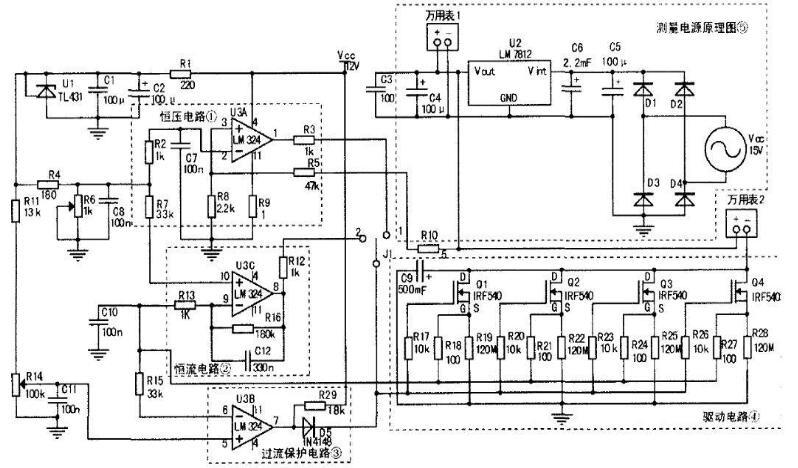
Multifunction Cutting Machine,Cutting Machine Pipe,Plastic Cutting Machine,Metal Cutting Machine

Kunshan Bolun Automation Equipment Co., Ltd , https://www.bolunmachinery.com