**LED Lamp Drive Power Circuit Diagram (a) - Circuit Working Principle**
The circuit of the LED corridor light is shown below. It consists of a capacitor step-down circuit, a rectifier circuit, an LED lighting circuit, and a photoelectric control circuit. The 220V AC power passes through capacitor C1 and resistor R1 to limit current, resulting in approximately 15V AC at points A and B. This voltage is then rectified by diodes VD1 to VD4, producing a DC voltage of about 14V across capacitor C2, which powers high-brightness LEDs VD5 to VD8 with a working current of around 14mA. Since capacitor C1 does not consume active power, the power consumed by the bleeder resistor is negligible, making the total power consumption of the circuit approximately 15 × 0.014 = 0.2W.
To further reduce power consumption and extend the lifespan of the high-brightness LEDs, a photoelectric control circuit composed of a photoresistor R2, resistor R3, and transistor VT1 has been added. At night, the resistance of R2 can reach 100kΩ or higher. The voltage across C2 is divided between R2 and R3, resulting in a very low DC bias voltage for the base of VT1, which keeps it in cutoff mode and has no effect on the LED operation. During the day, due to the photoelectric effect, the resistance of R2 drops below 10kΩ, turning on VT1 and bringing it close to saturation. This causes the voltage across C2 to drop below 4V due to the shunt current from VT1, effectively reducing power usage.
**LED Lamp Drive Power Supply Circuit Diagram (2) - Specific Requirements for LED Driver Power Supplies**
LEDs are low-voltage, long-life, high-efficiency, safe, and environmentally friendly light sources. For AC input power supplies, an isolated output is essential for safety. The higher the efficiency of the LED driver, the better, as it enhances the overall energy-saving performance of the LED. High switching frequency and efficiency also allow the driver to be compact, making it easier to integrate into small LED lamps. High constant current accuracy ensures consistent brightness and color when using LEDs in large quantities.
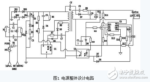
**Power LED Lamp Cup Application Scheme Below 10W**
Currently, power LEDs under 10W are widely used, with many integrated products available that combine the LED driver and the lamp in one unit, offering convenience for users. Common specifications include GU10, E27, and PAR30. We have designed the following scheme (see Figure 1):
**Key Features of the Design:**
1. Based on the latest LED driver chip AP3766, this design uses primary-side control without requiring an optocoupler or secondary-side current control, simplifying the circuit structure.
2. The AP3766 employs a proprietary "sub-micron startup current" technology, requiring only 0.6μA of startup current, improving system efficiency.
3. It features constant current tightening technology for precise current regulation.
4. The circuit uses a minimal number of components, with the AP3766 packaged in SOT-23-5, allowing easy installation in standard lamp cups.
5. It includes isolated output, open-circuit protection, overvoltage protection, and short-circuit protection.
6. The power switch tube is a transistor, eliminating the need for high-voltage FETs and reducing costs.
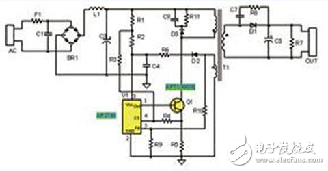
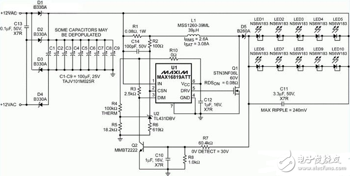
**LED Lamp Drive Power Circuit Diagram (3)**
This schematic shows a driver circuit for an AR111 LED with a 5S2P configuration. The MAX16819 operates in buck-boost mode, providing an average of 500mA per LED string. It drives a total of 10 LEDs arranged in 2 series and 5 parallel. The input voltage is 12VAC with ±10% tolerance. Schottky diodes D1-D4 form a full-wave rectifier, while capacitors C1-C8 filter the voltage. Some capacitors may be removed to reduce cost, depending on the application. Tantalum capacitors are used for their good temperature characteristics.
Since the LEDs are arranged in 5S2P, achieving perfectly matched currents is challenging. However, careful selection of the number of LEDs per string and the hybrid architecture helps minimize current differences.
**LED Lamp Drive Power Circuit Diagram (4)**
This design uses the TNY279 power chip as the core of the switching power supply. It integrates a 700V high-voltage MOSFET switch and a power controller. Unlike traditional PWM controllers, it uses a simple on/off control mode to stabilize the output voltage. The chip includes an oscillator, enable circuit, current limit regulator, 5.8V regulator, undervoltage/overvoltage protection, and overtemperature protection.
The core of the power supply is a flyback converter, known for its simplicity and ease of implementation. The overall circuit is shown in Figure 1.
**Input Rectification Filter Circuit**
To improve power factor and reduce harmonic distortion, a passive PFC circuit is used. Inductors L1 and L2, along with capacitors C1 and C2, form a π-type EMI filter. A valley filling circuit consisting of D1, D2, D3, C3, C4, and R3 reduces harmonics. The rectified and filtered DC voltage is applied to the primary winding of T1, while a clamp circuit formed by D4, C5, and R6 protects the drain voltage spike.
**High Frequency Transformer Design**
The TNY279 is self-powered, but the use of a bias winding allows for overvoltage protection in case of feedback failure. This design includes a bias winding, which enables the chip to be powered by a lower voltage, reducing no-load power consumption to less than 40mW.
**Feedback Circuit Design**
The secondary side uses a dual-loop control system with the NCS1002, which integrates a 2.5V reference and two precision op amps. One op amp controls the voltage loop, while the other manages the current loop. The current is detected through resistor R17 and compared with the reference to provide feedback to the TNY279 for adjustment.
**Working Principle**
When the output voltage exceeds the set value, current flows through the optocoupler LED, pulling down the transistor’s current. If this current exceeds the threshold, the next cycle is suppressed. Similarly, when the current on R16 exceeds the set value, the optocoupler pulls down the current, suppressing the next cycle. This feedback mechanism ensures stable output voltage and current.
In the event of a feedback failure, the internal latch shutdown circuit activates if the BP/M pin current exceeds ISD, protecting the load. Using the bias winding reduces no-load power consumption significantly.
**LED Lamp Drive Power Circuit Diagram (5)**
An LED driver is a power converter that provides the correct voltage and current to drive the LED. Inputs can include high-voltage AC, low-voltage DC, high-voltage DC, or low-voltage high-frequency AC.

Modern LED drivers often use electrolytic capacitors, which have limited lifespans. However, patented IC drivers eliminate the need for these capacitors, extending life to over 40,000 hours—ten times longer. These drivers are smaller, fitting into standard LED bulbs without changing the original design, making them user-friendly and cost-effective.
**LED Lamp Drive Power Circuit Diagram (6)**
A buck/boost converter is required when the input voltage is higher or lower than the total LED voltage. A circuit based on the LTC3783 drives eight 1.5A LEDs. The input range is 9–36V, with a total LED voltage of 18–37V. At VIN=14.4V, Vo=36V, and I0=1.5A, the output power is 54W with 93% efficiency. The switching frequency is set via resistor R5 (20kHz–1MHz). R7 and R8 set the overvoltage protection level, while R4 senses the LED current.
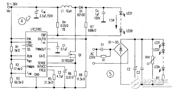
Flyback, SEPIC, and CUK topologies can all regulate input voltage up or down, but they are generally less efficient than buck-boost configurations. Each topology has unique advantages but is typically less efficient than the buck-boost design.
Multifunctional Power Meter,Power Meter,Multi-Function Ammeter,Multifunction Meter
zhejiangjinyidianqiyouxiangongsi , https://www.jooeei.com