Ask a question
Can I turn the RF source on or off within 200 ns?
In pulse radar systems, high power amplifiers (HPAs) must switch rapidly between transmit and receive modes. This typically requires a conversion time of less than 1 μs. Traditionally, this is done using drain control, which involves switching large currents between 28 V and 50 V. While effective, this method adds complexity, size, and potential reliability issues. In modern phased array systems, where size, weight, and power (SWaP) are critical, eliminating drain switches is highly desirable.
This article introduces a simple yet innovative gate pulse drive circuit that allows fast HPA switching without the need for a drain control circuit. The measured switching time is under 200 ns, with sufficient margin to meet the 1 μs target. Key features include programmable offset compensation, gate clamping to prevent voltage spikes, and overshoot control to optimize the pulse rise time.
Traditional Drain Pulse Configuration
A typical HPA configuration using drain control is shown in Figure 1. A series FET is used to switch the high voltage to the HPA’s drain. The control circuit must generate a higher voltage than the logic level to activate the FET. However, this approach presents several challenges, such as high current switching, the need for an additional discharge path when the FET is off, and the requirement for a higher voltage to turn on an N-channel FET.
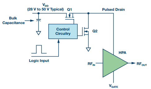
Figure 1. Traditional HPA pulse drain configuration
The main drawbacks of this setup include the need for low-inductance paths, the necessity of a separate discharge FET, and the difficulty of generating higher voltages for N-channel devices. These factors increase system complexity and SWaP, making it less ideal for modern phased array applications.
Recommended Gate Pulse Circuit
The proposed gate drive circuit converts a logic-level signal into a suitable gate control signal for GaN HPAs. It uses a negative bias to set the operating current and a more negative voltage to turn the device off. The circuit must also overcome gate capacitance, ensuring a fast rise time and minimal overshoot.
One key concern is that even a small increase in gate voltage can cause a significant rise in HPA current, so stability and clamping are essential. Additionally, different HPA devices may require varying bias settings, making in-system programmability beneficial.
The circuit in Figure 2 meets all these requirements. An operational amplifier is configured in an inverting mode with a single negative supply. The op-amp reference is set using a precision DAC, allowing precise control of the output voltage. When the logic input is high, the output is clamped to the negative rail, while a low input results in a small negative voltage. This design ensures the HPA turns on when the logic signal is low, minimizing unnecessary power consumption.
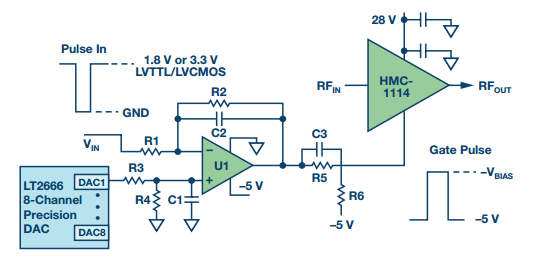
Figure 2. Recommended HPA gate drive circuit
Component values were carefully selected to ensure optimal performance. R1 and R2 set the gain, while R3 and R4 along with the DAC determine the reference voltage. C1 filters noise, and R5 and R6 provide clamping. C3 compensates for the gate capacitance, and C2 limits overshoot on the rising edge of the pulse.
Actual Test Data
The test setup involved evaluation boards for the DAC, op-amp, and HPA. A pulse generator simulated a 1.8 V logic signal, and an RF sampling oscilloscope measured the HPA's response. The results showed that the turn-on time was less than 200 ns, with a rise time of about 300 ns. The shutdown time was significantly faster, also under 200 ns, providing ample margin for system design.
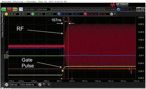
Figure 4. Measured HPA turn-on time
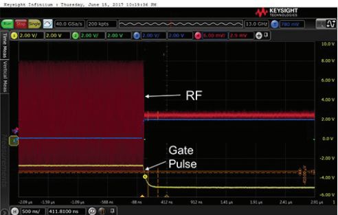
Figure 5. Measured HPA shutdown time
Layout Considerations
The layout in Figure 6 shows how the gate pulse circuit can be integrated into a phased array system. The op-amp section is placed close to the HPA input to minimize signal loss. The DAC is assumed to be in the control section, supporting multiple transmit channels. The layout demonstrates that the circuit can be implemented in a compact, low-cost PCB with minimal additional space required.
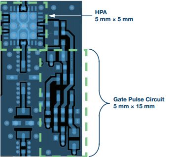
Figure 6. Physical size allocation
Conclusion
This paper presents a novel gate pulse circuit that enables fast HPA on/off switching without the need for traditional drain control. Key benefits include sub-200 ns switching, compatibility with any logic input, programmable offset compensation, gate voltage clamping, and optimized rise time. The design supports high-density phased array applications and offers a scalable solution for future systems requiring rapid RF switching.
Super Tweeter Bullet,Tweeter Driver,Speakers For Concert Speakers,Speakers For Performances
NINGBO RFUN AUDIO TECHNOLOGY CO.,LTD , https://www.mosensound.com