introduction
Broadband Low Noise AmpliTIer (BBLNA) is a key component of receiving systems such as communication, measurement and control. Its noise figure, gain and frequency response characteristics directly affect the main performance of the receiving system. Therefore, in the field of wideband receiving systems, the design of wideband low noise amplifiers will have a very broad market prospect. The power gain of various low-noise devices decreases with increasing frequency and decreases by approximately 3~5 dB per octave. In order to obtain a wider and flatter frequency response characteristic, the gain roll-off must be compensated. However, intentionally reducing the gain of the low frequency band necessarily causes the input and output standing wave ratios to deteriorate, and the noise figure will also become larger. However, for wideband low noise amplifiers, it is generally not possible to use isolators to improve the standing wave ratio. In addition, the input and output impedance of low-noise devices also vary greatly with frequency, which increases the complexity of the matching circuit. Although the circuit structure of the wideband low noise amplifier has many forms, the balanced amplifier designed with the Lange coupler has the noise advantage, and its noise figure is similar to that of the single-ended low noise amplifier, and can be completely designed when designing the matching circuit. According to the optimal noise matching design, it is not necessary to balance the input and output standing wave ratios. Therefore, a balanced circuit structure is selected for the design of a wideband low noise amplifier.
1 Design principle
The balanced wideband low noise amplifier consists of two low noise devices and two Lange couplers. The two low noise devices and their matching circuit networks are identical, which reduces the computational complexity of the matching circuit, input and output standing waves. Good ratio, low noise, working frequency band up to 1~2 octave.
2 Lange coupler
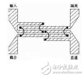
The Lange coupler, also known as the 90° three-decibel bridge, has a schematic structure as shown in Figure 1. It has outstanding advantages over other couplers in terms of wideband and tight coupling characteristics. The design idea is to use several coupling lines parallel to each other, so that both sides of the line are coupled to achieve tight coupling, and the bandwidth is improved by compensating the phase velocity. Almost all commonly used microwave circuit simulation software has a typical model to facilitate the design.
3 Design principles
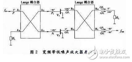
The schematic diagram of the balanced wideband low noise amplifier is shown in Fig. 2. If the power and phase of the input RF signal fin are P and 0°, respectively, it is divided into two parts P1 and P2 by the Lange coupler. P1 phase is -90° and P2 phase is -180°, which are amplified by two paired low noise devices. Since the matching circuit is the same, the gain G is the same, the transmission phase shift is changed by 180°, and the amplified two signals are GP1, GP2, GP1 phase is -270°, and GP2 phase is 0°. After the two signals are synthesized by the coupler, the GP1 and GP2 are equal in size and the phase difference is 180°, and there is no power output. In the B1 port, GP1 and GP2 have the same phase, and the two parts are superimposed and output fout, and the size is GP1+GP2. =G(P1+P2)=GP. That is, under ideal conditions, the gain of a balanced wideband low noise amplifier is equal to the gain of a single low noise device.
The use of a balanced circuit structure has the following advantages:
(1) Since each low-noise device only undertakes half of the power amplification, the amplifier output power 1 dB compression point will increase by 3 dB, the corresponding dynamic range will also increase by 3 dB, and the third-order intermodulation will be improved by about 6 dB.
(2) The port standing wave ratio is greatly improved. Now it is assumed that the reflection coefficients of V1 and V2 are equal. The RF signal fin is input by the coupler A1 port, and is equally divided into two parts, which are output by A2 and A3 ports, and the reflected power of the A2 port is returned. To the A1 port, the total path phase shift is -180°; the reflected power of the A3 port returns to the A1 port, and the total path phase shift is -360°. Obviously, the two parts of the reflected power are equal in magnitude and opposite in phase, thus canceling, so on the A1 port. There is no reflected power. In addition, the reflected power of V1 and V2 is superimposed on the A4 port, and it is necessary to add 50 Ω to match the load RL for absorption. Through the phase shifting action of the coupler, the port standing wave ratio is ideally constant at 1.
(3) The stability of the amplifier operation is improved, and the determination conditions of the amplifier stability are as follows:
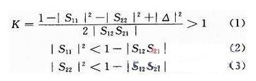
Where: Δ = S11S22-S12S21, K is the stability factor. When the above three conditions are met at the same time, the amplifier is absolutely stable. It can be proved that the stability coefficient K of the balanced amplifier is constant greater than 1. In Fig. 2, the A1 port and the B1 port are theoretically non-reflective, and there is no self-oscillation due to reflection of the signal source or the load. Although a single low-noise device itself has potential instability in the low frequency band, as long as the matching circuit is well designed, the A1 port and the B1 port are absolutely stable. This feature is important in wideband reception systems, especially when the antenna is matched to the amplifier.
(4) The lowest noise figure of the balanced amplifier is basically the same as that of the single-ended amplifier, but when designing the matching circuit, the optimal noise matching design can be completely adopted to obtain the ideal minimum noise matching without having to balance the standing wave ratio.
In the narrow-band low-noise amplifier, the common structure of the DC bias power supply lead-in is λg/4 high-impedance microstrip line, and the terminal uses a fan-shaped line or a capacitor to short-circuit the high-frequency. The available working frequency band of this structure is up to 40%. ~50% bandwidth. Therefore, in the wideband low noise amplifier circuit, it is impossible to use this type of bias lead-in line, and the microstrip line center jumper type bias lead-in line can be used, that is, the jumper is soldered on the microstrip center axis. In the ideal state, there is no electric field distribution in the space directly above the center of the microstrip line. The distance between the outer solder joints of the jumper and the edge of the microstrip is at least greater than the thickness of the substrate to ensure that the solder joint is outside the electric field. Since the diameter of the jumper has a weak influence on the inductance, the length has a great influence on the inductance and needs to be accurately controlled. The jumper can be properly removed from the surface of the substrate to reduce the effect of the floor on the inductance. Also consider the low frequency filtering of the power supply and the interstage low frequency decoupling capacitors. The decoupling and bypass circuits should be large enough to avoid low frequency oscillations. The DC-blocking capacitors in the microstrip circuit should use high-bandwidth, high-stability temperature coefficient, non-resonant and low-loss wide-band surface-mount capacitors, such as the DLI C06 series. The lateral width of the shielding box should be less than half the wavelength of the highest operating frequency to avoid the waveguide transmission effect in the internal space of the casing. The microstrip substrate should be well grounded, and the number of fixing screws should be relatively large. It is preferable that the hole walls of the screw holes are metallized. During commissioning, the corresponding frequency band absorbing material is applied to the inner surface of the upper cover of the casing to reduce the in-band gain fluctuation caused by the spatial coupling.
The broadband low-noise amplifier also needs to be designed for electromagnetic compatibility. First, the power supply line entering the shielding box is filtered using a feedthrough capacitor with a feedthrough filter to reduce crosstalk caused by the power line. Secondly, the amplifier needs to be solved. The port matching ensures that the integration is compatible with the receiving system; finally, electromagnetic shielding measures are required for the box to reduce the interference caused by electromagnetic radiation. Strengthening electromagnetic compatibility work during the research and development phase is beneficial to the product passing the corresponding standard electromagnetic compatibility test.
In this range,including Rotary Switch,Door Switch , Push Button Switch, 303 Cord-Line Switch and so on.
Rotary Switch is mostly used in the cooler area,according to different requirement,many function can be met.For example,4 Position,6 Position,3 Position etc.
High Quality and Reseasonal Price,it is very popular.
Push Switch,Toggle Switches,Led Push Switch,Push Button Switch
Ningbo Kara Electronic Co.,Ltd. , https://www.kara-switch.com