The conditional access system (CAS) of digital television is part of the program authorization and management for digital television users and is one of the important components of digital television broadcasting. The use of an open card separation structure is an important future development trend of the conditional access system. The card separation is to separate the universal TV reception system suitable for mass production from the private CAS management system by defining a general physical interface and related interface communication protocol on the user receiving terminal. At present, the international implementation of the card separation mode is implemented by using a physical interface similar to the PCMCIA socket on a portable computer. The standard published by the European DVB organization is called DVB-CI, and the United States has a similar standard called POD. In fact, the definitions of these two interfaces have been included in the new PCMCIA standard documentation. The PCMCIA card in which the loading condition receives the processing content is simply referred to as a digital television conditional receiving card, and may be simply referred to as a CAM (Conditional Receiving Module).
This article refers to the address: http://
In fact, the establishment of the standard for separation of machine cards, after opening a standard socket on the TV, is not only to solve the problem of public viewing and private management, but its great significance will also be reflected in the figures as consumer goods. TVs have a way to upgrade performance and expand functionality. Just like the current development scale of PCs, it has an inseparable relationship with the standardization of interfaces such as ISA, PCI, and APG of PCs. It is hard to imagine whether the industry could achieve such great success if the computer does not have a standardized and expandable interface. In the field of digital television, the development of the standard for separation of machine cards and the opening of standard interfaces on digital TV sets will introduce digital TV into a colorful development field. For example, for different program signal transmission methods (wireless broadcasting, cable, satellite, digital audio broadcasting), you can insert different types of receiving modules on the CI interface (machine card separation universal interface); for us in digital The photos saved on the camera memory card can be browsed on the TV through a universal memory card reader module; through the broadband IP receiving module, the various streaming programs on the network can be enjoyed on the TV and the two-way transmission of the network can be performed; The module connects the TV set with other electrical devices into a home digital network system; through the hard disk video recording module, the user can record programs with license certification and the like. The trend and potential of its development will be more difficult to predict in the future.
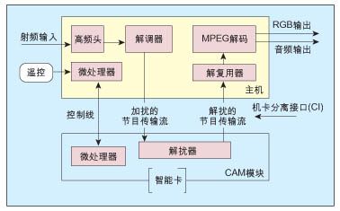
Figure 1: Schematic diagram of the separation mechanism of the machine card.
The structure of CAM can generally be based on a high-performance 32-bit SoC chip, with smart card interface, CI interface, dedicated TS transport stream processing engine, DVB universal descrambling and other components. CAM card space is very limited, but to achieve a high-speed 32-bit embedded system that can process HDTV program streams, so the size and performance of its core SoC chip has become a key point.
Through our intensive research on DVB-CI standards in Europe, combined with our own product development experience in embedded products and integrated circuits, we have successfully developed the performance and integration of SoC technology based on ARM7TDMI. The international leading CAM chip SM1658 also greatly reduced the production cost of CAM and eliminated the price bottleneck of large-scale promotion of the separation standard of machine cards.
CAM structure and hardware system
The SM1658 is a typical dedicated embedded microprocessor for CAM systems. It integrates all the main functional modules of a CAM. The CAM structure with its core is very simple.
The SM1658 uses the widely popular 32-bit ARM7TDMI as the CPU core. In addition to the common circuit modules such as memory management, interrupt controllers, timers, watchdogs, asynchronous serial communication, and PLL, the integrated SoC chip is also internal. It integrates 256KB high-speed SRAM, smart card interface, PCMCIA (DVB-CI) interface, high-speed TS stream demultiplexing/filtering engine and DVB universal descrambler. The basic structure is shown in Figure 1. Only one external FLASH program memory chip is needed to form a high-performance CAM card.
The memory management module of SM1658 can support a total of 4 memory segments. This memory portion can be internal or external SRAM or external FLASH. The data line width and read/write speed of each memory can be initialized by software. The maximum capacity of each memory segment can support up to 4M bytes, and the four memory segments can support up to 16M bytes. Among them, the memory implemented inside the chip is 256KB high-speed internal SRAM, which can execute the core program of the system at high speed without waiting cycle, greatly improving the processing capability of the key program of the chip.
The SM1658's interrupt controller provides 32 channels of interrupt management. Each interrupt can select priority level, trigger up/down edge, pulse/level trigger selection, and provide rich interrupt management features such as interrupt masking, interrupt reservation, and soft trigger. The CI physical interface is a subset of the PCMCIA standard. Can be divided into TS stream channel and command channel. Our CI interface is fully compliant with the DVB-CI interface standard and provides bidirectional buffering, CIS memory and flexible status and control registers on the hardware architecture.
Three 16-bit timers are also provided internally, each with a selectable 8-bit prescaler. The watchdog of the chip is 32-bit. If the watchdog is not needed, it can be configured as a 32-bit timer.
design feature
1. Simple and efficient local bus
In SoC design, the choice of internal and external bus is a very important factor. An efficient and compact bus can improve the efficiency and scalability of the chip.
In the SoC chip design of the ARM architecture, ARM generally recommends using the standard AMBA bus for design. At the same time, the ARM7TDMI core itself comes with a simple internal bus. Before deciding on the bus specification used, we performed the following analysis of the architecture and application characteristics of the SM1658.
One of the advantages of the AMBA bus is its ability to support calls, rulings, and data flow of multiple master devices. In the SM1658, there is only one master device ARM7TDMI, the other module circuits are in the slave device state, and the CPU is uniformly scheduled, and all the external slave devices use the same clock as the master device, and can immediately respond to the CPU access in a single clock. . Therefore, using ARM7 local bus in this aspect is more advantageous.
If you use the AMBA bus, the design team can use a large number of third-party IP modules that are compliant with the AMBA bus specifications and are rigorously verified. In the chip design of the SM1658, in order to minimize the cost of the chip, and objectively, because important module circuits do not have the proper IP, we have designed all the circuit modules ourselves. Then, the development time that you want to save by using IP is not feasible.
In addition, if you use the AMBA bus, you must add a first-stage pipeline to the original ARM7TDMI's three-stage pipeline, and convert the bus structure of the ARM7TDMI's dual-clock edge to a single clock-edge bus structure, which simplifies the post-chip design. the amount. However, this results in a loss of one clock cycle for some jump instructions, reducing the CPU's operating efficiency. In addition, using the AMBA bus, the CPU and each module need to increase the interface logic of the AMBA bus, increasing the size and cost of the chip.

Figure 2: Basic structure of the SM1658.
Finally, we decided to adopt the ARM7TDMI's own local bus from the perspective of the maximum efficiency of the chip and the simplified logic control. The use of ARM7's local bus has several advantages: ARM7's local bus state is relatively simple, does not require relatively complex AMBA bus protocol verification; low interface requirements for the module, interface circuit is very simple; reduce the pipeline length, at the highest In a SoC chip in which the clock is fixed by an IP hard core, the reduction in the flow rate means that the code execution efficiency of the chip is improved. At the same time, strict constraints and verification of the double-edge clock problem on the ARM7 bus ensure the correctness of the chip's later design.
2. Internal SRAM with software redundancy
ARM7TDMI is a CPU core without internal cache. It can only wait for idle SRAM and FLASH memory. Even with the high-speed external SRAM, the full performance of the high-speed CPU cannot be effectively used due to the data interface width and the delay of data transfer between the chip and the chip. At the same time, the large-capacity high-speed SRAM is expensive and will greatly increase. The cost of the CAM system. In terms of system structure and cost, we decided to embed a 256KB SRAM in the SM1658. This SRAM capacity can meet the application requirements of a considerable number of CAM systems. At the same time, our chips also support a variety of external high-speed and low-speed SRAM, for some systems with very large SRAM requirements can also meet the requirements.
The SRAM implemented inside the SM1658 has very high performance, and can complete ARM's various instructions in a single clock cycle, that is, the CPU does not need any wait when fetching or accessing data in the internal SRAM. After the chip is produced, we use the SRAM inside the chip to test the CPU performance. Even at very high frequencies, the chip can obtain the same level as the theoretical calculation value of the ARM core of the ARM7TDMI, followed by the test data. form.
The biggest problem with embedded SRAM is that it has an impact on the yield of the chip. We have taken some effective precautions in circuit function design, low-level software design and application system, greatly reducing the system's dependence on defective SRAM. In this way, the yield of the chip can be greatly improved. This also reduces the overall cost of the chip from a system perspective.
3. Dynamically adjustable clock circuit
In the clock design of the SM1658 chip, we also integrated a software-configurable clock management circuit called dynamic clock circuit. We program the clock processing module of the chip through software, which can make the working clock frequency of the chip change continuously as needed, reduce the power consumption of the chip under light task load, and can adapt to the input of various external clock sources, and increase the CAM. The adaptability of the system in product development.
4. Highly flexible smart card interface
Among the features of the SM1658 is a highly flexible smart card interface. It is to ensure that CA can authorize and manage programs for users to watch through smart cards.
In general, most smart card interfaces in the world are interconnected according to the ISO7816 standard. In many SoC chip designs, everyone uses an external smart card interface chip. For example, TDA8004 is a commonly used smart card interface chip. However, with an external chip, the reliability of the system will be reduced and the cost will be higher. We hope to design a system with the best cost and performance, and completely omit the external interface chip through the circuit design.
First of all, in the design of this interface module, all the states and control methods are completed according to the ISO7816 standard. For example, the design of different power supply electrical requirements for Class A and Class B smart cards; the design of error handling for the T0 communication protocol and other communication protocols; and the special protocol requirements for certain private smart cards. These can be done by configuring the driver software on the chip with a small number of simple external devices. Secondly, we designed different external circuits to match the internal control of the chip for the ESD requirements of the smart card interface and the differences in different usage environments. At the same time, we have independently configured the logic characteristics of each interface pin of the chip under different conditions, which can minimize the requirements on external circuits.
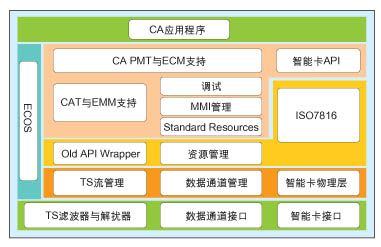
Figure 3: Functional block diagram of the smart card module system software.
In standard use, the SM1658 chip can perform smart card interface functions without any external active components, and the ESD resistance can be guaranteed to be greater than 4,000V.
5. Embedded high-speed DVB universal descrambling algorithm
The universal scrambling algorithm is a standard scrambling algorithm recommended for the TS stream by the DVB standards organization. Currently, this algorithm is commonly used in digital broadcasting programs in Europe. In China's current commercial CA, the scrambling of TS programs is basically the same algorithm. Therefore, we applied to the DVB organization for authorization of this algorithm and embedded it in our SM1658 chip in a solid-core mode.
In the design of this solid core, the chip's adaptability to multi-channel high-definition programs that may appear in the future is fully considered. The processing capability of the descrambling module is designed to be 175 Mbps, which can simultaneously process 2 channels of high-definition program streams or 4 road signs clear programs. The level of flow.
6. High-performance TS stream processing engine
In SM1658, we also designed a TS stream processing engine to shape, filter, extract specific data, and send back the descrambled program stream to the TS stream transmitted from the CI interface. In this engine, we designed 64 PID filters and 16 SECTION filters. According to different configuration states, this engine can complete 7 different routing functions for TS streams.
SM1658 performance index
Maximum working clock frequency
The SM1658 chip is manufactured using SMIC's 0.18um standard logic CMOS process. In the chip design of the SM1658, we used ARTISAN's 0.18um process library and MC compiler, integrated with SYNOPSYS's DC synthesis tool, and used the latest CADENCE back-end design tool ENCOUNTER for layout and SI analysis. The chip's internal bus, memory and critical path modules are optimized so that the timing of the chip essentially meets the standard performance tested on the ARM7TDMI IP core manual.
After the tape was completed, the chip was tested for the highest clock frequency. With a core voltage of 1.8V and a IO voltage of 3.3V at room temperature, the SM1658 can operate at a frequency of 125MHz to 135MHz, which may be the highest operating frequency of the commercially available ARM7TDMI type chip.
Since we optimized the bus and internal memory of the chip, we want to confirm this optimization effect. We benchmarked the highest computing power of the chip. Our test program uses the reference test program Dhrystone 2.1 (written in C) provided by ARM to compile in the most optimal way. The test program runs in the chip's internal SRAM. The table below compares our test results with the results of the software simulation test. It can be seen that the performance of our chip at the highest performance has basically reached the best indicator of ARM7TDMI, which also shows that our design is very optimized.
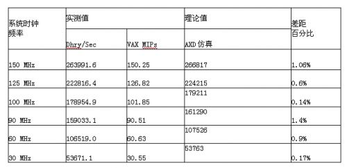
Table 1: The highest computing power benchmark results for the SM1658.
2. Current consumption
Since a large-capacity SRAM and a high-speed PLL are embedded inside the chip, the main current consumption of the chip during operation will be generated. In the design, the state of power consumption is also fully considered, and the SRAM is decomposed into a plurality of independent parts, so that only one part of the SRAM is working at the same time. Through circuit management and optimization, the average power consumption when the chip runs the program at full speed is as follows:
Brief introduction to the software system
For any SoC chip, the software design, development and application system is an indispensable part of its commercialization. From the very beginning, we designed a SM1658 chip and organized a software development team to develop the SM1658 software. In the design process of the chip, the software group is designed synchronously. After the chip completes the design flow, our software underlying, application development platform and some application software have been basically completed.
Here is a brief introduction to the software architecture of the SM1658. The software architecture of the SM1658 can be divided into two major parts: the API library (application programming interface) and the application. The API is similar to the API library under WINDOWS. It completes some basic and dedicated function libraries (including the basic function functions of the OS system) required for all drivers and upper software development related to the chip hardware. Users can compare them based on the API library. Conveniently set up user applications.
The API library can be further divided into an underlying hardware driver function library, a basic application service function library, and an advanced application service function library. The underlying drivers of the SM1658 include basic devices such as timers, watchdogs, memory management, interrupt management, serial port and other devices. They also include dedicated smart card interfaces, machine card separation CI interfaces, and TS stream processing engine drivers. The physical drive of the device. The function of the underlying driver is to complete the initial configuration of the device, the change of the working state, the transmission and reception check of the basic data packet, the handshake with other devices, the processing of the error state, and the basic processing work closely related to the hardware.
The basic application services include management of TS stream processing status, management of CI command channel data, and implementation of the underlying protocol of the smart card, including the underlying management functions of the OS system. It provides some relatively low-level functions, users can use these functions to call, to control the working state of the chip in more depth and carefully. You can also optimize the performance of certain application tasks for some special cases in your application.
The advanced application service implements resource management of specific devices, user display interface MMI management, management of CAT and EMM data, application interface of smart card, and high-level management functions of the OS system. It provides some comparison of upper layer or abstract function calls. By calling these functions, the user can perform tasks and functions relatively simply, allowing the user to focus on building the content of the application system.
In the API library of the software system, two sets of communication protocol interfaces are also completely implemented, which are respectively the DVB-CI protocol and the 7816 protocol of the smart card. Users directly use the upper-level functions of these protocols, which greatly simplifies the software development workload when designing CAM cards.
In terms of operating system, we have adopted a very flexible ECOS as the operating system of this embedded system. The ECOS system is powerful, but has a very convenient and customizable configuration mode, which is especially suitable for the system and future expansion modes. Since the current CAM does not require file management and no GUI interface, after the ECOS is configured for this chip, its OS core code is only about 50 KB.
Conclusion of this paper
As part of the digital TV communication segment, CAM also has an important feature of Content Protection and Copy Management (CPCM). Since the transparent program stream caused by the separation of the machine card appears on the interface, which is not conducive to the copyright protection of the program product, a copy protection mechanism must be added between the set top box and the CAM.
- These lights look like many beautiful fire flies, and the copper wire is extra flexible, You can decorate teenager or girls 's rooms to enjoy ambience of relaxing, decorate your wedding to memorize your important and romantic moment, decorate it in restaurant or shop, create welcome feeling, customers will be attracted by the twinkle String Lights,walk into shop or restaurant, stay longer, enjoy their commodity or food and love your shop or restaurant.
- You can also decorate your party to feel more joyful, decorate holidays and Christmas to enjoy happy times.With extra flexible copper wire, you can put these led starry string lights in the glass jar,vase, or you can easily bend and shape it around wreaths, trees, flowers, and almost everything else.
Battery Led String Lights,Led String Lights,Outdoor String Lights,Solar Led String Lights
Dongguan Xingyong Indusrtial Co,Ltd , http://www.xingyongled.com