The origin of the level standard:
In the digital communication process in the format of high (1) and low (0), the analog voltage values ​​corresponding to high and low are inevitably involved, and the determination of this value is reason and historical. Specifically, it relates to the development of semiconductor devices, such as TTL, Transistor-Transistor Logic, because the first invention in semiconductor devices is a bipolar transistor. Then, due to the development of MOS, the CMOS process has brought new changes to the power supply requirements of the circuit, resulting in changes in the output digital level standard.
First, TTL and CMOS level introduction
The TTL circuit can only work at 5V or below, when VCC=5V.
TTL output: VOH>2.4V, VOL<0.4V.
Input: VIH>2.0V, VIL<0.8V.
The CMOS circuit has a wider operating voltage range of 12V and VCC=5V.
CMOS output: VOH > 4.99V, VOL <0.01V.
Input: VIH>3.5V, VIL<1.5V.
It can be seen that the noise margin of the TTL level is 0.4V, and the noise margin of the CMOS is 1.5V.
TTL and CMOS gate structure:
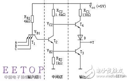
As shown in the TTL gate structure, the output stage uses a push-pull output structure, and T4 is in the form of an emitter follower. The output resistance is small and the load capacity is strong.
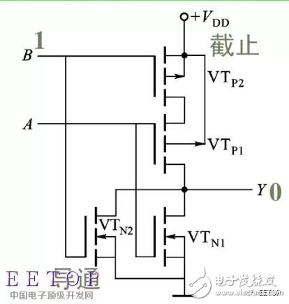
As shown in the CMOS gate structure.
Several features of TTL and CMOS drivers:
1, TTL output resistance is small, so the load capacity is generally stronger.
2, TTL response speed is generally in the ns level, CMOS is slightly larger, but the advanced high-speed MOS design speed is not lost to TTL.
3. TTL is driven by current, which consumes more power and cannot be integrated on a larger scale.
4. The CMOS gate input is more susceptible to interference because the input impedance is much larger than the TTL input and therefore cannot be left floating.
5, the modern integrated circuit technology integrated TTL and CMOS features developed Bicmos process.
6, TTL and CMOS levels are different, need to be converted in order to effectively identify.
Development of TTL and CMOS levels
Because there is a free interval between the high level of TTL of 2.4V and 5V, and later developed a low voltage LVTTL, the specific level standard according to the manual.
3.3V LVTTL: VCC: 3.3V VOH>2.4V, VOL<0.4V; VIH>2V; VIL<0.8V;
V2.5V LVTTL: VCC: 2.5V. VOH>2.0V, VOL<0.2V, VIH>1.7V, VIL<0.7V.
LVCMOS levels have also been developed.
3.3V LVCMOS: Vcc: 3.3V; VOH>=3.2V; VOL<=0.1V; VIH>=2.0V; VIL<=0.7V. 2.5V LVCMOS: Vcc: 2.5V; VOH>=2V; VOL<=0.1V; VIH>=1.7V; VIL<=0.7V.
Second, high-speed level standards
How to achieve high-speed drive output in high-speed circuits? Either increase the drive current, either lower the level standard or increase the transistor operating speed. Obviously the former will bring very large power consumption, so changing the level standard and improving the transistor design becomes an option. Although the low level is more susceptible to interference, a stricter hardware design is required.
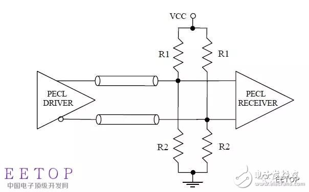
1, ECL and PECL level interface
ECL, Emitter Coupled Logic, uses a differential structure output and requires a negative supply. Later, the development of PECL, that is, positive power emitter coupling logic. The basic principle is to use the transistor to work in the unsaturated zone to reduce the conversion time and greatly improve the conversion speed.

The output of the ECL always has current through it, which is very beneficial for high speed conversion. The output impedance is a few ohms, the output current is about 10 mA, and the driving capability is strong.
Interface connection: DC coupling, suitable for short distances
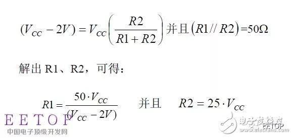
This matching method is equivalent, and the specific resistance is calculated:

Interface connection: AC coupling, suitable for longer distances


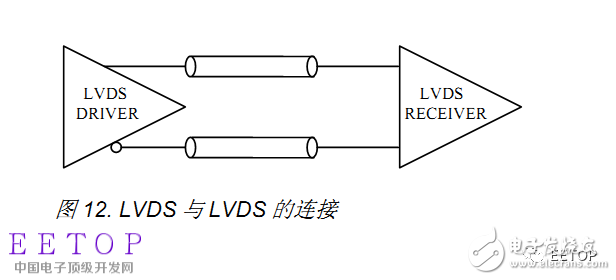
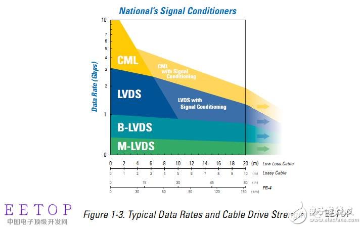
2, LVDS level interface
LVDS, Low-Voltage Differential Signaling, is a level standard for transmitting high-speed signals using low-voltage differential signals. Features: low voltage, low power consumption, strong noise suppression.
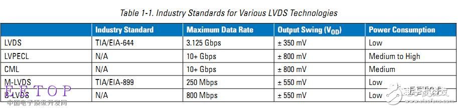
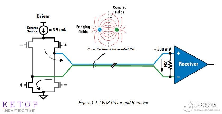
Figure LVDS input and output specifications:

LVDS connection method: direct connection, because there is a termination resistor in the chip.
 ,
,
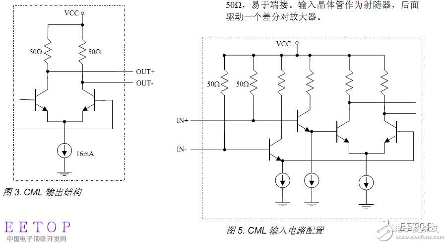
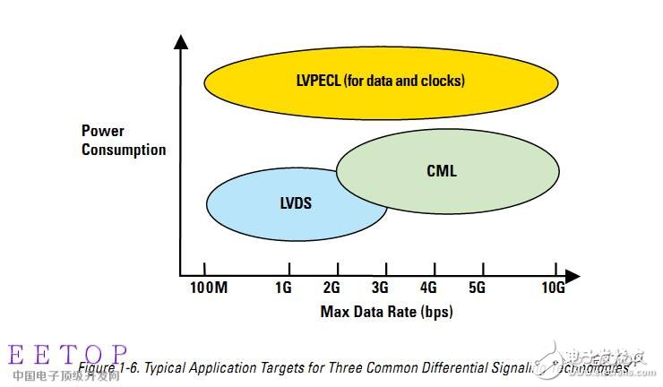
Third, CML level interface
CML is the current mode logic level, which uses constant current drive and built-in matching resistor. It is easy to use and has the longest range of short-distance high-speed applications.
The following figure is a simple comparison of the performance of several high-speed interfaces:
Third, common common level standards
The most widely used in the industrial field should be the 485 232 level standard. Both have advantages and disadvantages, low cost and simple use, but there are still many technical points that can be discussed, such as transmission speed, distance, protection design and so on.
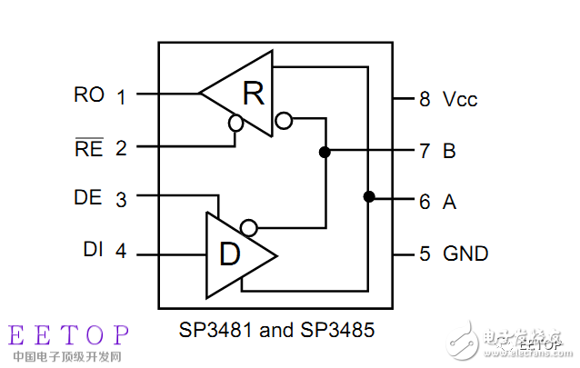
Because the 485 output is an A/B differential signal, 485 is a half-duplex communication, and 232 is a full-duplex communication.
Several features and reasons for 485 and 232:
1, transmission distance. Affected by the drive capacitance, 232 allows a capacitive load of 2500pF, so the transmission distance is 15~30m. The 485 uses differential transmission, and the distance can reach up to kilometer.
2. Transmission reliability. 232 Because the transceiver is more susceptible to interference due to the common ground, 485 can actually be applied to two lines, and the reliability is better.
3. Level standard. 232: The high level is -3V~-15V. The low level is +3V~+15V. When 485 is sent: the high level AB is +2V~+6V, the low level is -2V~-6V, and the difference of |AB| is more than 200mV when receiving.
4. Regarding the common mode level, it is obvious that the common mode level of 232 is higher, which is easy to damage the chip, and the reliability is slightly lower.
5, RS485 can carry out networking communication, the bus can carry up to 32 units.
RS232 and RS485 protection design instructions:
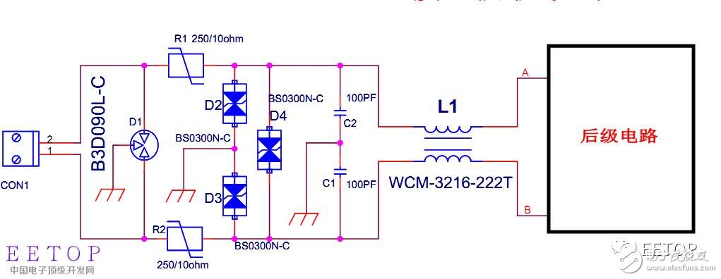
The protection design problem of the interface has always been the top priority. The basic circuit structure principle is actually not difficult, mainly due to the comprehensive analysis and processing of the problem. Step by step according to the interference source-propagation path-shielding measures. As shown in Figure 485, the interface protection circuit design
RS232 and RS485 connection problems:
At work, I learned that many students have been confused about the connection of 232 or 485. Regarding the definition of the transceiver and the connection of the male and female heads, I often felt puzzled at first. The main line is to send and receive the three lines.
The standard 232 is the DB9 connector:
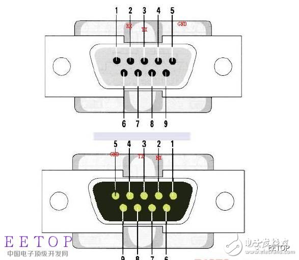
A brief note is: 235-receiving land.
485 how to use DB9 connection:
The two lines of 485 correspond to the 1, 2 feet of the DB9 head.
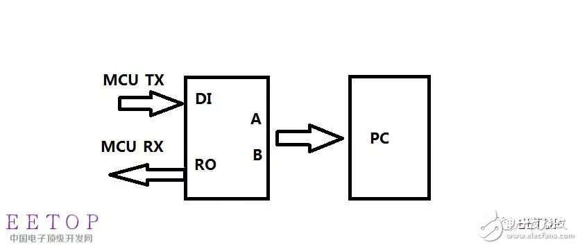
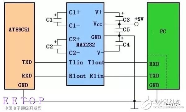
232 and 485 connections to the MCU:
Fourth, summary
There are mainly several standards for digital levels. These are defined at the hardware level. In software, there are various protocols for communication methods. The interface design is indeed the focus of circuit design, especially in the current high-speed digital communication applications, I think there are several main aspects to be mastered:
1. The application circuit of the signal level, that is, the basic structure should be clear.
2, protection design issues should be considered comprehensively, different interfaces for load requirements for matching degrees are not the same.
3, the importance of PCB design, in the high-speed design, many use EDA software simulation to help find the problem of interference, but the first thing to do is to strictly follow the relevant rules and specifications to design.
4. The necessity of the experiment. Especially for the interference problem of the interface, the most comprehensive experimental design is one of the best ways to solve the problem as soon as possible.
In short, the theoretical basis must be, design considerations must be, test experiments must be full, and so, the results may be good!
ZGAR MINI
ZGAR electronic cigarette uses high-tech R&D, food grade disposable pod device and high-quality raw material. All package designs are Original IP. Our designer team is from Hong Kong. We have very high requirements for product quality, flavors taste and packaging design. The E-liquid is imported, materials are food grade, and assembly plant is medical-grade dust-free workshops.
From production to packaging, the whole system of tracking, efficient and orderly process, achieving daily efficient output. We pay attention to the details of each process control. The first class dust-free production workshop has passed the GMP food and drug production standard certification, ensuring quality and safety. We choose the products with a traceability system, which can not only effectively track and trace all kinds of data, but also ensure good product quality.
We offer best price, high quality Vape Device, E-Cigarette Vape Pen, Disposable Device Vape,Vape Pen Atomizer, Electronic cigarette to all over the world.
Much Better Vaping Experience!


ZGAR Vape Pen,Disposable Device Vape Pen,UK ZGAR MINI Wholesale,ZGAR MINI Disposable E-Cigarette OEM Vape Pen,ODM/OEM electronic cigarette,ZGAR Mini Device
ZGAR INTERNATIONAL(HK)CO., LIMITED , https://www.zgarvapor.com