(This article is contributed by Texas Instruments, author BrettBarr of Texas Instruments) This article will discuss how to select MOSFETs (metal oxide half field effect transistors) for hot swapping.
When the power supply and its load are suddenly disconnected, the large current swing on the parasitic inductance of the circuit will produce a huge spike voltage, which will have a very adverse effect on the electronic components on the circuit. Similar to battery protection applications, here MOSFETs can isolate the input power from other circuits. But at this time, the role of the FET is not to immediately disconnect the input and output, but to reduce the serious consequences of the destructive surge current. This requires a controller to adjust the gate-source bias voltage on the MOSFET between the input voltage (VIN) and the output voltage (VOUT), so that the MOSFET is saturated, thereby preventing the current that may pass (see Figure 1).
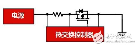
Figure 1: Simplified hot swap circuit
The first thing to consider for FET is to choose an appropriate breakdown voltage, which is generally 1.5 to 2 times the maximum input voltage. For example, 12V systems are usually 25V or 30VFETs, while 48V systems are usually 100V or in some cases 150VFETs. The next consideration should be the safe operating area (SOA) of the MOSFET, such as a curve in the data sheet. It is particularly helpful to indicate how the MOSFET affects thermal breakdown during short-term power surges, which is no different from what must be absorbed in hot-swap applications. Since the safe operating area (SOA) is the most important criterion for proper selection, please refer to Understanding the MOSFET Data Sheet-SOA Diagram. This article details how TI performs the measurement and then generates the SOA of the MOSFET shown in the device data sheet.
For designers, the key question is how large the maximum surge current the FET may experience (or is expected to be limited to the output) and how long this surge will last. Knowing this information, it is relatively easy to find the corresponding current and voltage difference on the SOA diagram of the device data sheet.
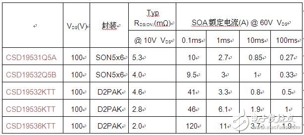
For example, if the design input voltage is 48V and wants to limit the output current to no more than 2A within 8ms, the designer can refer to the 10ms curve of CSD19532KTT, CSD19535KTT and CSD19536KTTSOA (Figure 2) and infer that the latter two devices may work. The CSD19532KTT does not work. Because CSD19535KTT already has enough margin, for this kind of application, the more expensive CSD19536KTT may provide too high performance.
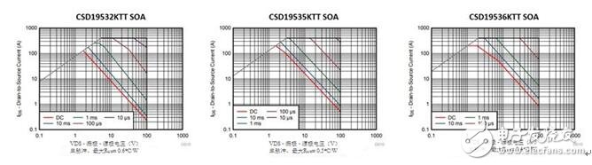
Figure 2: SOA of three different 100VD2PAKMOSFETs
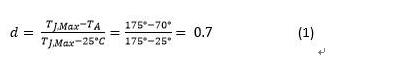
Assume that the ambient temperature is 25ËšC, which is the same as the SOA measurement on the data sheet. Since the final application may be exposed to a hotter environment, the SOA must be derated proportionally based on the ratio of the ambient temperature to the maximum junction temperature of the FET. For example, if the maximum ambient temperature of the final system is 70ËšC, the SOA curve can be derated using Equation 1:
In this case, the 10ms, 48V capability of the CSD19535KTT will drop from ~2.5A to ~1.8A. It is deduced that a particular FET may no longer be suitable for this application, so designers should choose CSD19536KTT instead.
It is worth noting that this method of derating assumes that the MOSFET fails exactly at the maximum junction temperature, although this is usually not the case. Assuming that the failure point measured in the SOA test actually occurs at 200ËšC or any other higher temperature, the calculated derating will be closer to uniform. In other words, the calculation of this derating method is not a conservative algorithm.
SOA will also determine the type of MOSFET package. D2PAK packages can accommodate large silicon chips, so they are very popular in higher power applications. The smaller 5mm×6mm and 3.3mm×3.3mm quad flat no-lead (QFN) packages are more suitable for low-power applications. In order to withstand surge currents less than 5-10A, FETs are usually integrated with the controller.
Here are a few points to note:
When targeting hot-swap applications, designers can use the same SOA selection process for any situation where FETs work in the saturation region, even for OR-ing applications, Power over Ethernet (PoE), and low-speed switching applications (such as motors). Control) Using the same FET selection method, a very high overlap of VDS and IDS will occur during the MOSFET turn-off period.
Hot swapping is an application that tends to use surface mount FETs instead of through-hole FETs (such as TO-220 or I-PAK packages). The reason is that the short pulse duration and heating of the thermal breakdown event are very limited. In other words, the capacitive thermal resistance element from the silicon junction to the case can prevent heat from quickly dissipating to the circuit board or heat sink to cool the junction. The function of chip size-the thermal impedance from junction to case (RθJC) is important, but the function of the package, circuit board and system heat dissipation environment-the thermal impedance from junction to ambient (RθJA) is much smaller. For the same reason, it is difficult to see heat sinks used in these applications.
Designers often assume that the lowest resistance MOSFET in the catalog will have the strongest SOA. The logic behind this is-lower resistance in the same silicon wafer production usually indicates a larger silicon chip inside the package, which does produce better SOA performance and lower junction-to-case thermal resistance. However, with the renewal and iteration of silicon wafers increasing the resistance per unit area (RSP), silicon wafers also tend to increase cell density. The denser the cell structure inside the silicon chip, the more likely the chip is to undergo thermal breakdown. This is why older generation FETs with higher resistance sometimes also have better SOA performance. In short, it is necessary to investigate and compare SOA.
Please learn more about various hot-swappable controllers on TI's official website. Table 1-3 at the end of this article highlights some of the devices used for hot swapping, and they provide some reference values ​​for SOA functions.
For more information, please refer to the MOSFET Options blog series.
Table 1: MOSFETs for 12V hot swap
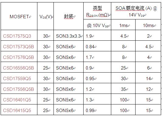
Table 2: MOSFETs for 24V hot swap
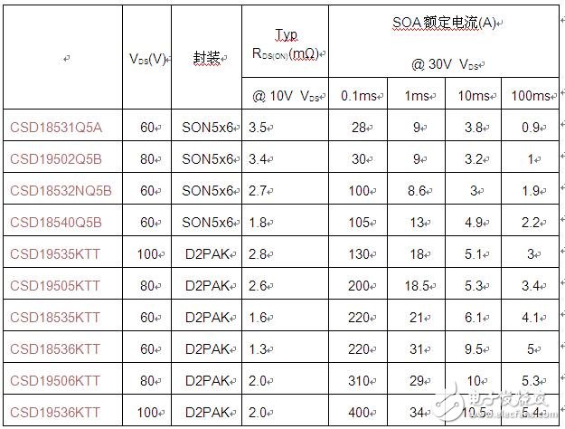
Table 3: MOSFETs for 48V hot swap
Other capacitors
Other Capacitors,Ac Filter Capacitor,Power Saver Capacitor,Line Filter Capacitor,Low Voltage Capacitor
YANGZHOU POSITIONING TECH CO., LTD. , https://www.cnfudatech.com